Display panel and manufacturing method thereof

A technology for a display panel and a manufacturing method, which is applied to electrical components, electrical solid-state devices, circuits, etc., can solve problems such as the falling off of the circuit layer in the binding area, and achieve the effects of good adhesion performance, improved reliability, and avoidance of loosening.

Pending Publication Date: 2022-04-12
SHENZHEN CHINA STAR OPTOELECTRONICS SEMICON DISPLAY TECH CO LTD
View PDF0 Cites 0 Cited by
  • Summary
  • Abstract
  • Description
  • Claims
  • Application Information

AI Technical Summary

Problems solved by technology

[0003] The embodiment of the present application provides a display panel and a manufacturing method thereof, so as to solve the problem that the wiring layer of the binding area of ​​the existing display panel falls off

Method used


Image

  • Display panel and manufacturing method thereof
  • Display panel and manufacturing method thereof
  • Display panel and manufacturing method thereof

Examples


Embodiment Construction

[0038] The technical solutions in the embodiments of the present application will be clearly and completely described below in conjunction with the drawings in the embodiments of the present application. Apparently, the described embodiments are only some of the embodiments of this application, not all of them. Based on the embodiments in this application, all other embodiments obtained by those skilled in the art without making creative efforts belong to the scope of protection of this application.

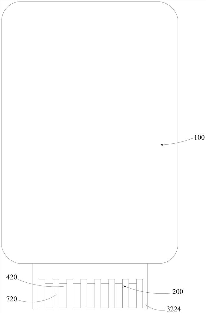
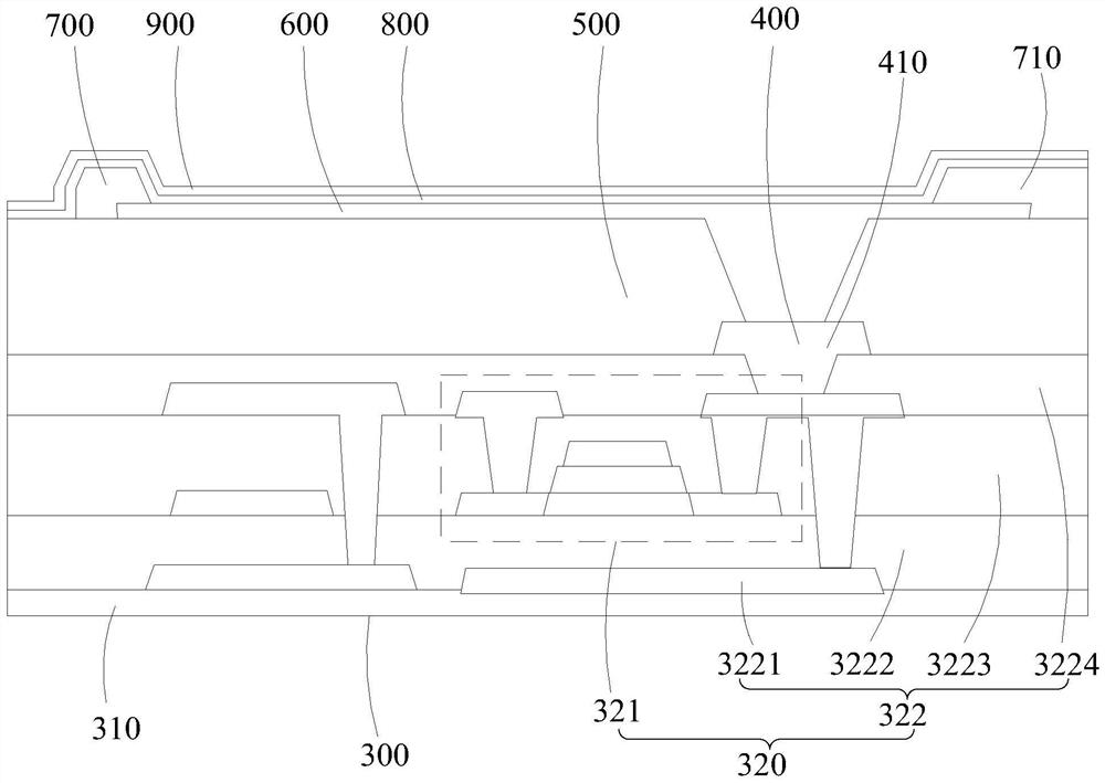
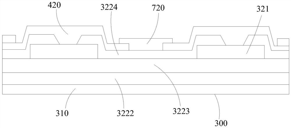
[0039] Embodiments of the present application provide a display panel and a manufacturing method thereof, so as to solve the problem that the wiring layer of the binding area of ​​the existing display panel falls off. It will be described below in conjunction with the accompanying drawings.

[0040] In order to illustrate the structure of the display panel more clearly, the display panel will be introduced below with reference to the accompanying drawings.

[0041] Exemplary, s...


PUM


Abstract

The invention provides a display panel and a manufacturing method thereof.The display panel is provided with a display area and a binding area, the display panel comprises a substrate, a circuit layer, a flat layer, an anode, a pixel definition layer, a light-emitting layer and a cathode, the substrate comprises a second insulating layer, the circuit layer is arranged on the second insulating layer, and the flat layer is arranged on the second insulating layer; the circuit layer comprises a circuit pattern arranged in the display area and a plurality of connecting wires, the connecting wires extend to the binding area from the circuit pattern, the pixel definition layer comprises a plurality of pixel retaining walls arranged on the flat layer and a plurality of bonding retaining walls arranged in the binding area, one part of each bonding retaining wall is pressed on the edge of the corresponding connecting wire, and the other part of each bonding retaining wall is pressed on the edge of the corresponding connecting wire. And the other part is pressed on the second insulating layer. The bonding retaining wall is arranged on the pixel definition layer, so that the reliability of the circuit layer in the binding area is improved, and the problem that the circuit layer in the binding area falls off is greatly solved.

Description

technical field [0001] The present application belongs to the field of display technology, and in particular relates to a display panel and a manufacturing method thereof. Background technique [0002] In the current production of medium and large size OLED products, due to the direct contact between the PAD layer (circuit layer, made of MoTi and other materials) and the PVS layer (insulation layer, made of organic materials) in the film layer design of the binding area, the two One is an inorganic film layer and the other is an organic film layer, so the adhesion between them is poor. Because the PAD layer is located on the outermost surface and is in a bare state, if the adhesion between the PAD layer and the PVS layer is not good and there is no other film protection at the boundary of the contact surface, it is easy to fall off. Especially when the OLED display panel is reworked, the PAD layer in the binding area is prone to obvious peeling off. This problem will direct...

Claims


Application Information

Patent Timeline
Patent Type & Authority Applications(China)
IPC IPC(8): H01L27/32
Inventor 刘超凡
Owner SHENZHEN CHINA STAR OPTOELECTRONICS SEMICON DISPLAY TECH CO LTD
Why Eureka
Try Eureka