Substrate bonding apparatus and substrate bonding method
A bonding device and bonding method technology, applied in semiconductor/solid-state device components, semiconductor/solid-state device testing/measurement, semiconductor devices, etc., can solve problems such as difficult maintenance, complex installation, and reduced efficiency, and improve space utilization. rate, prevent coordinate errors, and reduce unqualified effects
- Summary
- Abstract
- Description
- Claims
- Application Information
AI Technical Summary
Problems solved by technology
Method used
Image

Examples
Embodiment Construction
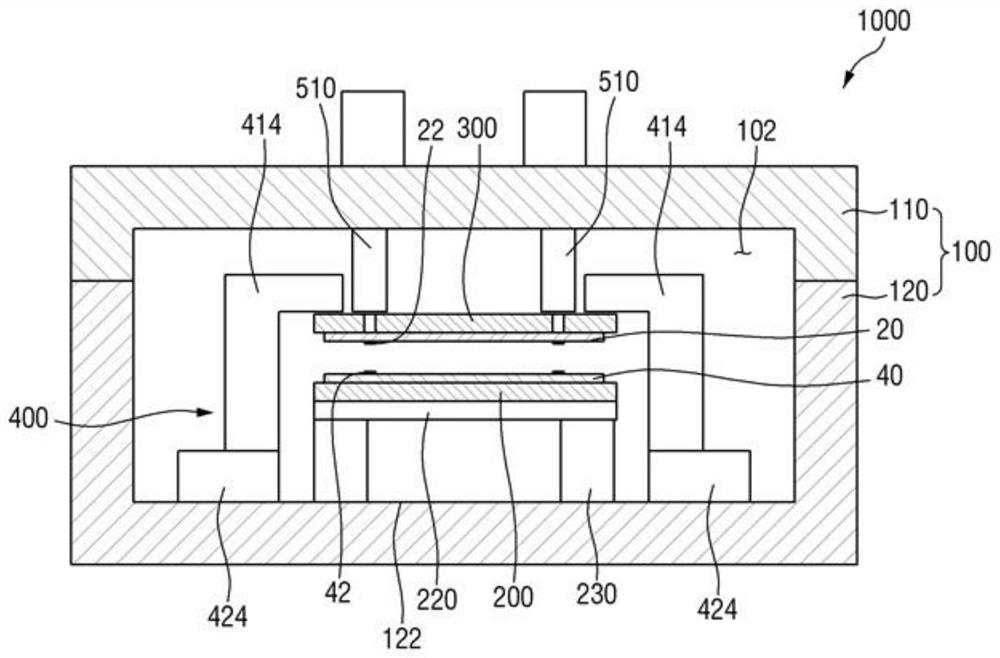
[0048] Hereinafter, the configuration of the substrate bonding apparatus 1000 according to the embodiment of the present invention will be specifically described with reference to the drawings.
[0049] figure 1 It is a side cross-sectional view of a substrate bonding apparatus 1000 according to an embodiment of the present invention.
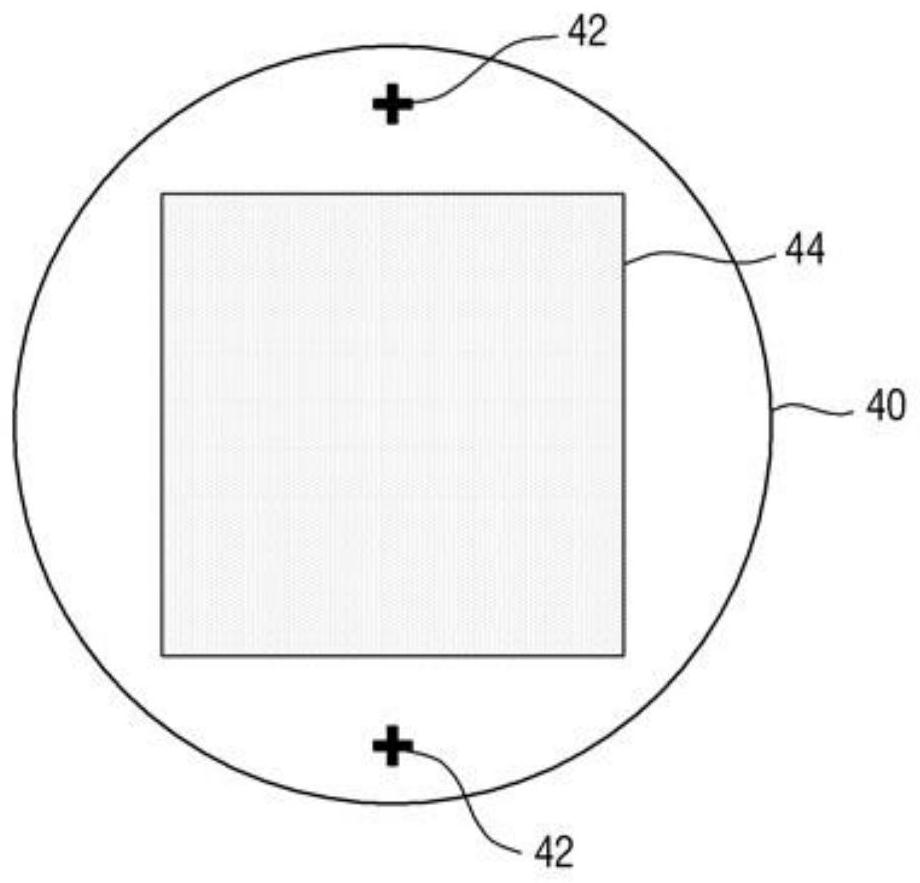
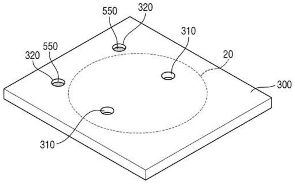
[0050] refer to figure 1 , the substrate bonding apparatus 1000 has: a cavity 100 ; a first chuck 200 arranged inside the cavity 100 to adsorb the first substrate 40 ; a second chuck 300 to face the first chuck 200 It is arranged inside the cavity 100 and can move relative to the first chuck 200 in the vertical and horizontal directions to adsorb the second substrate 20 ; and the camera 510 is located in the first chuck 200 and the second chuck 200 . Either side of the upper and lower parts of the chuck 300 is used to identify the first sorting key 42 of the first substrate 40 and the second sorting key 22 of the second substrate 20 .
[0...
PUM
 Abstract
Description
Claims
Application Information
 - R&D Engineer
- R&D Manager
- IP Professional
- Industry Leading Data Capabilities
- Powerful AI technology
- Patent DNA Extraction
Browse by: Latest US Patents, China's latest patents, Technical Efficacy Thesaurus, Application Domain, Technology Topic.
© 2024 PatSnap. All rights reserved.Legal|Privacy policy|Modern Slavery Act Transparency Statement|Sitemap