Board splicing process and device for circuit board production

A circuit board and jigsaw technology, which is applied to the assembly of printed circuits with electrical components, printed circuits, and printed circuit manufacturing. The effect of structural strength

Pending Publication Date: 2022-07-12
LONGNAN JUNYA ELECTRONICS TECH CO LTD
View PDF0 Cites 0 Cited by
  • Summary
  • Abstract
  • Description
  • Claims
  • Application Information

AI Technical Summary

Problems solved by technology

[0005] The purpose of the present invention is to provide a kind of jigsaw device for circuit board production, to solve the test board and production board proposed in the a

Method used


Image

  • Board splicing process and device for circuit board production
  • Board splicing process and device for circuit board production
  • Board splicing process and device for circuit board production

Examples


Example Embodiment

[0033] In order to make those skilled in the art better understand the technical solutions of the present invention, the present invention will be further described in detail below with reference to the accompanying drawings.

[0034] The present invention provides such as Figure 1-5 A paneling process and device for circuit board production shown, wherein a paneling process for circuit board production includes the following steps:

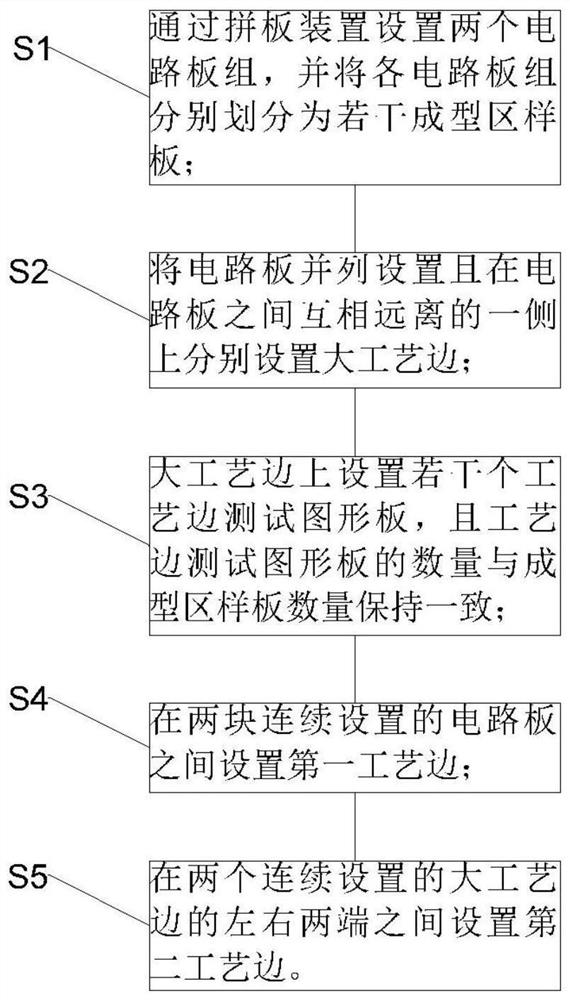
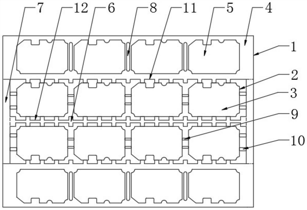
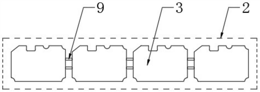
[0035] S1. Set up two circuit board groups through a jiggering device, and divide each circuit board group into several molding area templates;

[0036] S2, arranging the circuit boards side by side and setting large process edges on the sides of the circuit boards away from each other;

[0037] S3. A number of process edge test graphics boards are set on the large process edge, and the number of process edge test graphics boards is consistent with the number of samples in the molding area;

[0038] S4, setting a first process edge between two...


PUM


Abstract

The invention discloses a board splicing process and device for circuit board production, and relates to the field of circuit board production, and the board splicing device for circuit board production comprises a board splicing whole body, the board splicing whole body is provided with two circuit board groups, the two circuit board groups are horizontally arranged in parallel, and the two circuit board groups are arranged on the board splicing whole body. Each circuit board group comprises a forming area pattern template, the sides, away from each other, of the two circuit board groups are connected with large process edges, the large process edges are provided with process edge test pattern plates, and a first process edge is arranged between the two circuit board groups. The process edge test pattern board corresponding to the forming area pattern template is arranged on the large process edge, so that the forming area pattern template and the process edge test pattern board are designed on the same circuit board, the overall size of the jointed board is kept unchanged, the overall utilization rate of the jointed board is greatly improved, accurate test of patterns is realized, and the production efficiency is improved. And the yield of products is greatly ensured.

Description

technical field [0001] The invention relates to the field of circuit board production, in particular to a jiggering process and device for circuit board production. Background technique [0002] The assembly of the circuit board refers to the assembly of some irregular unit modules after the circuit board completes the customer unit design, so as to reduce the waste of PCB boards. The panel design needs to combine the processing capabilities of the various process equipment of the PCB factory, refer to the size specifications of the sheet, and design a panel that can meet the manufacturer's optimization of the quality of the board, the lowest production cost, the highest production efficiency, and the highest utilization rate of the board. size. The process side of the circuit board assembly refers to the part that is added to the two sides or four sides of the PCB board in order to assist the production of the plug-in board, and the welding wave crest is mainly used to ass...

Claims


Application Information

Patent Timeline
IPC IPC(8): H05K3/36H05K3/00
CPCH05K3/36H05K3/0097
Inventor 沈书亮余华赖康明许观成
Owner LONGNAN JUNYA ELECTRONICS TECH CO LTD
Why Eureka
Try Eureka