
Collaborative processing device for multiple layers of PCBs (printed circuit boards)

A technology of PCB board and processing device, applied in the field of multi-layer PCB board collaborative processing device, can solve the problems of inconvenient and stable drilling, inconvenient for board body cleaning, inconvenient for multi-layer PCB board combined processing or sub-board processing, etc. It is easy to clean the board body and facilitate the effect of stable punching.

Pending Publication Date: 2022-07-29
江西奔特科技有限公司
View PDF1 Cites 2 Cited by
  • Summary
  • Abstract
  • Description
  • Claims
  • Application Information

AI Technical Summary

Problems solved by technology

[0004] The mechanism in the above-mentioned patent is convenient for punching exactly the same positioning holes on the four corners of multiple groups of PCB boards, which saves the transfer process of punching and lamination operations, but it is not convenient for combined processing or sub-board processing of multi-layer PCB boards. Yes, it is not convenient for stable punching, and it is not convenient for board cleaning

Method used


Image

  • Collaborative processing device for multiple layers of PCBs (printed circuit boards)
  • Collaborative processing device for multiple layers of PCBs (printed circuit boards)
  • Collaborative processing device for multiple layers of PCBs (printed circuit boards)

Examples


Embodiment Construction

[0034] In order to facilitate the understanding of the present invention, the present invention will be described more fully hereinafter with reference to the related drawings. Several embodiments of the present invention are given in the drawings, but the present invention can be implemented in different forms and is not limited to the description in the text. rather, these embodiments are provided so that this disclosure will be thorough and complete.

[0035] It should be noted that when an element is referred to as being "fixed" to another element, it may be directly on the other element or intervening elements may be present, and when an element is referred to as being "connected" to another element, it may be The terms "vertical," "horizontal," "left," "right," and similar expressions used herein are for the purpose of illustration only.

[0036] Unless otherwise defined, all technical and scientific terms used herein have the same meaning as commonly associated by one o...


PUM


Abstract

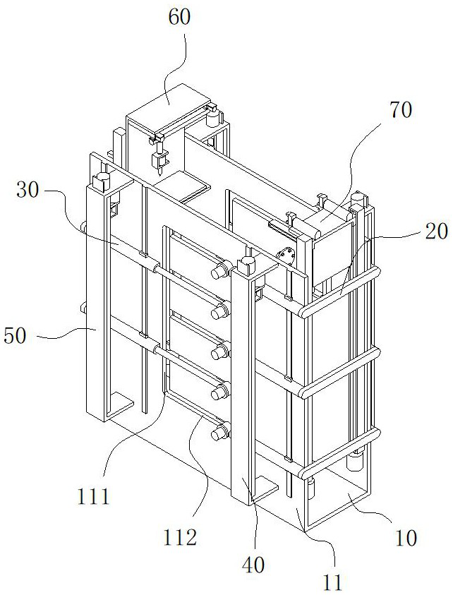
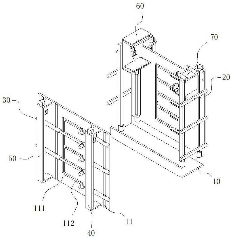
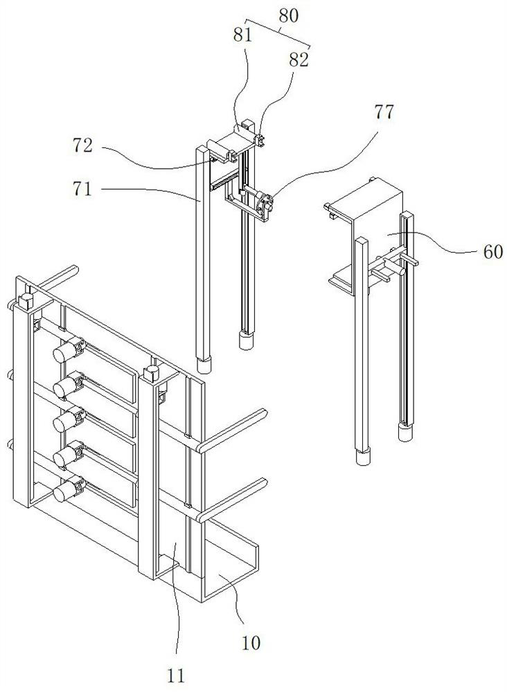
The invention discloses a multi-layer PCB collaborative processing device which comprises a base plate and two vertical plates, the outer walls of the two vertical plates are sequentially provided with a plurality of first PCB positioning devices and second PCB positioning devices from top to bottom, the first PCB positioning devices and the second PCB positioning devices are distributed in a staggered mode, and the side walls of the vertical plates are provided with first lifting driving devices and second lifting driving devices correspondingly. A drilling device and a plate body cleaning device are arranged between the two vertical plates; the first driving cylinder and the second driving cylinder are arranged at the two ends of the cross rod and slidably connected with the outer walls of the two vertical plates respectively, the rotating component is arranged at the executing end of the first driving cylinder, the telescopic component is arranged at the executing end of the second driving cylinder, and the executing end of the rotating component penetrates through the horizontal long hole to be connected with the first PCB positioning clamping plate. The execution end of the telescopic component penetrates through the horizontal long hole and is connected with the second PCB positioning clamping plate. According to the processing device, combined processing or split board processing of the multi-layer PCB is facilitated, stable punching is facilitated, and the board body is convenient to clean.

Description

technical field [0001] The invention mainly relates to the technical field of PCB board processing, in particular to a multi-layer PCB board collaborative processing device. Background technique [0002] The multi-layer PCB needs to be drilled when the multi-layer PCB is processed. When the multi-layer board is turned at the same time, the resistance of the drill bit will increase, which will affect the drilling effect. When drilling, burrs will be generated between the board layers. Burrs are not easy to remove. [0003] According to the collaborative processing method of multi-layer PCB boards provided by the patent document with the application number of CN202111368200.9, the method includes the following steps: S1, PCB board positioning: first prepare the raw materials of the PCB boards to be processed, and then combine the three groups of PCB boards. In order to be placed on the surface of the PCB board preset platform, and the overall horizontal displacement of the PC...

Claims


Application Information

Patent Timeline
Patent Type & Authority Applications(China)
IPC IPC(8): H05K3/00H05K3/26
CPCH05K3/0047H05K3/26H05K2203/0165H05K2203/1509H05K2203/1563
Inventor 肖海生
Owner 江西奔特科技有限公司
Learn More