Supercharge Your Innovation With Domain-Expert AI Agents!

Gate electrode and froming method thereof

A gate electrode and gate oxide film technology, which is applied in the field of gate electrodes, can solve the problems of fluorine atom penetration, increase in the thickness of the gate oxide film 12, and deterioration of the electrical properties of the gate oxide film 12.

Inactive Publication Date: 2004-10-20
HYUNDAI ELECTRONICS IND CO LTD
View PDF0 Cites 0 Cited by
  • Summary
  • Abstract
  • Description
  • Claims
  • Application Information

AI Technical Summary

Problems solved by technology

As a result, the thickness of the gate oxide film 12 increases, and the electrical characteristics of the gate oxide film 12 deteriorate significantly.
[0009] On the other hand, when tungsten silicide is formed on amorphous silicon, the grain size of the formed amorphous silicon is larger than that of polycrystalline silicon, but since the size of these grains is as small as 0.5 μm, fluorine atom penetration still occurs when forming tungsten silicide question

Method used


Image

  • Gate electrode and froming method thereof
  • Gate electrode and froming method thereof
  • Gate electrode and froming method thereof

Examples


Embodiment Construction

[0020] Hereinafter, preferred embodiments of the present invention will be described in detail with reference to the accompanying drawings.

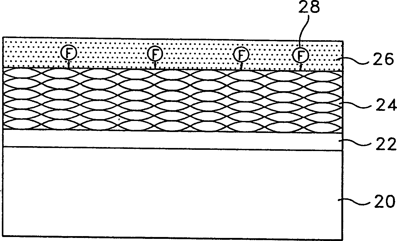
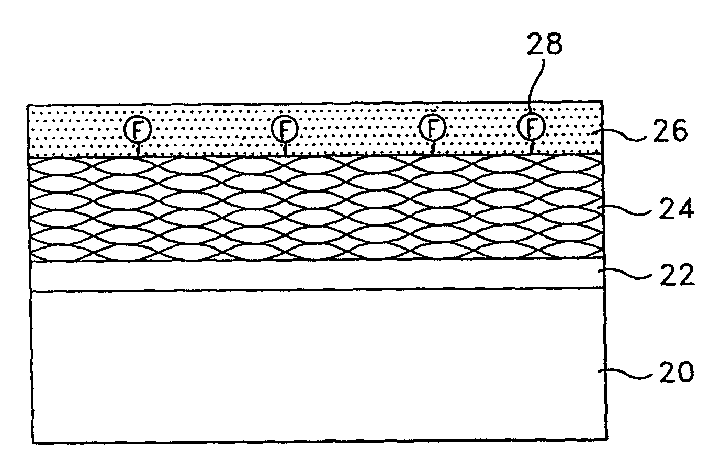
[0021] refer to figure 1 A gate insulating film 22 is formed on the upper portion of the semiconductor substrate 20, and an amorphous silicon layer 24 containing large structural grains and a tungsten silicide layer 26 containing a small amount of fluorine atoms are stacked on the upper portion of the gate insulating film 22.

[0022] With disilane (Si 2 h 6 ) as the source gas, the amorphous silicon layer 24 is formed by chemical vapor deposition, and its structure grain size is about 2-3 μm, compared with the existing structure of crystalline silicon stacking, its grain size is 10 times larger degree. Therefore, in the amorphous silicon layer 24, the impurity penetration path to the gate insulating film 22 side can be reduced to at least 1 / 10 compared with the conventional polysilicon layer used for the gate electrode. As a result...


PUM

PropertyMeasurementUnit
Particle sizeaaaaaaaaaa

Abstract

A gate electrode which has a structure in which a tungsten silicide layer is formed on an amorphous silicon layer is disclosed. A gate insulation film is formed on a semiconductor substrate, an amorphous silicon layer is formed on the gate insulation film by using disilane gas, and a tungsten silicide layer is formed on the amorphous silicon layer containing trace amounts of foreign matter. The grain size of the amorphous silicon layer is such that the foreign matter cannot enter the gate insulation film.

Description

technical field [0001] The invention relates to a gate electrode of a transistor used in a semiconductor device, in particular to a gate electrode with a tungsten silicide structure laminated on amorphous silicon. Background technique [0002] Generally, a gate electrode of a MOS transistor is formed on a semiconductor substrate on which a gate insulating film is formed first, prior to a source electrode and a drain electrode. The gate electrode is formed of polysilicon, and in order to improve its performance, either it is replaced by amorphous polysilicon, or a tungsten silicide layer is stacked on the polysilicon. [0003] figure 2 This is a conventional example, and is a partial cross-sectional view of a semiconductor element having a structure in which tungsten silicide is laminated on a polysilicon layer. [0004] see figure 2 , the existing gate structure is to form a gate oxide film (SiO 2 ) 12, stacking a polysilicon layer 14 and a tungsten silicide layer 16 seq...

Claims


Application Information

Patent Timeline
IPC IPC(8): H01L27/085H01L21/28H01L29/49H01L29/78
CPCH01L21/28052H01L29/4933H01L27/085
Inventor 崔在成
Owner HYUNDAI ELECTRONICS IND CO LTD
Features
  • R&D
  • Intellectual Property
  • Life Sciences
  • Materials
  • Tech Scout
  • Unparalleled Data Quality
  • Higher Quality Content
  • 60% Fewer Hallucinations
Learn More