Touch sensor wiring body, touch sensor wiring substrate, and touch sensor

A technology of touch sensor and wiring, which is applied in the direction of instrumentation, computing, and electrical digital data processing, etc. The effect of characteristic deterioration

Inactive Publication Date: 2017-11-28
THE FUJIKURA CABLE WORKS LTD
View PDF9 Cites 2 Cited by
  • Summary
  • Abstract
  • Description
  • Claims
  • Application Information

AI Technical Summary

Problems solved by technology

However, in the touch sensor of the above-mentioned technology, if the thickness of the transparent polymer layer between the conductive layer of the first layer and the conductive layer of the second layer of the wiring body is thin, the following disadvantages will occur. In the case of body contact, the released lines of electric force are also closed between the electrodes, making it difficult to react to the contact body
As a result, deterioration of electrical characteristics such as a decrease in sensitivity is caused, and further, it may not be able to function as a wiring body having a double conductive layer.
On the other hand, if the distance between the two-layer conductive layers is increased, the above-mentioned deterioration of the electrical characteristics is less likely to occur, but the film thickness becomes thicker, which hinders the reduction in weight and thickness.

Method used


Image

  • Touch sensor wiring body, touch sensor wiring substrate, and touch sensor
  • Touch sensor wiring body, touch sensor wiring substrate, and touch sensor
  • Touch sensor wiring body, touch sensor wiring substrate, and touch sensor

Examples


Embodiment 1

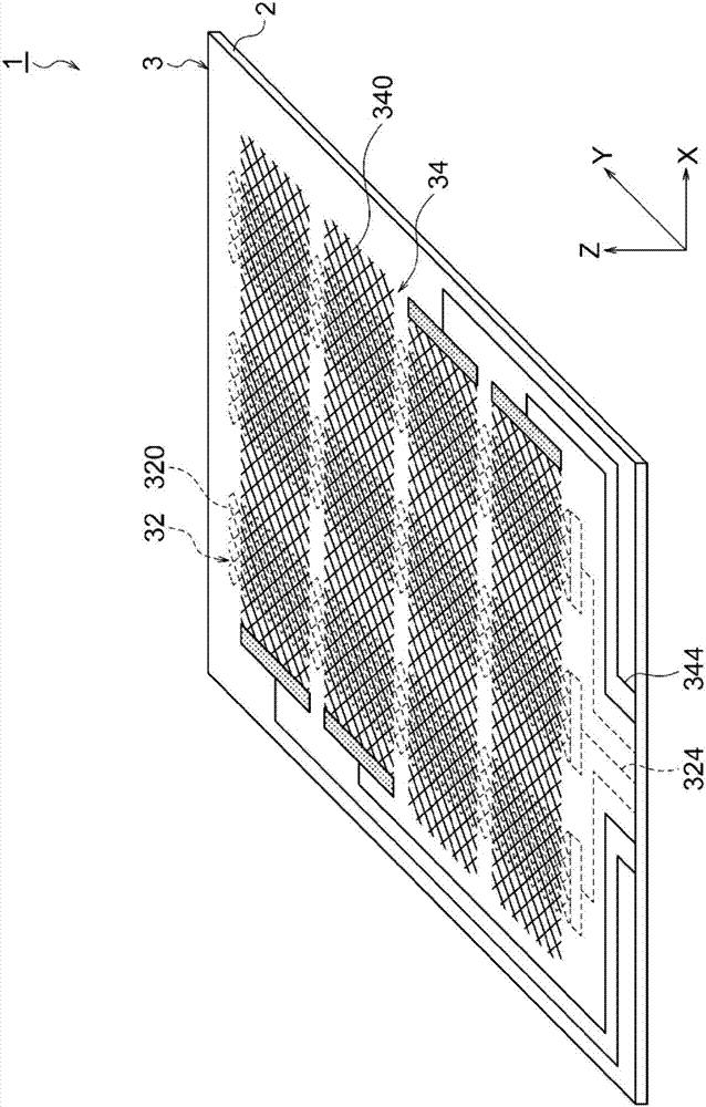
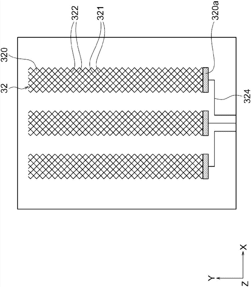
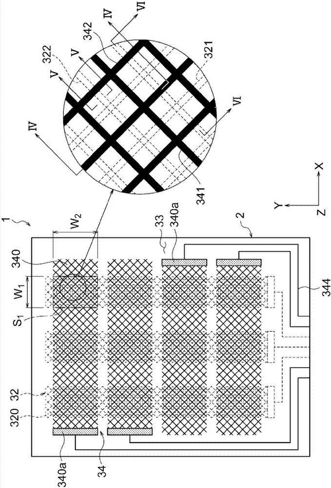
[0174] In Example 1, made Figure 1~4 The wiring board 1 for a touch sensor is shown. At this time, the thickness of the substrate 2 was formed to be 75 μm. The line width of the first conductor lines 321 and 322 constituting the first electrode pattern 320 of the first conductor layer 32 was 2 μm, and the line width of the lead 324 was 10 μm. The same applies to the second conductor layer 34 , and the line width of the second conductor lines 341 and 342 constituting the second electrode pattern 340 is 2 μm, and the line width of the lead 344 is 10 μm. The height (thickness) T of the first conductor line 321, 322 1 Formed to 3 μm. Similarly, the height (thickness) of the second conductor lines 341 and 342 is also formed to be 3 μm. As the substrate 2, a PET film was used, and as the conductive material 5, a thermosetting silver (Ag) paste was used. D as the first resin layer 31 1 The thickness is formed to be 15 μm, as the D of the second resin layer 33 2 The thickness ...

Embodiment 2

[0177] In Example 2, except that D of the second resin layer 33 2 The thickness was formed to be other than 25 μm, and a test sample was prepared in the same manner as in Example 1.

Embodiment 3

[0179] In Example 3, except that D of the first resin layer 31 1 The thickness was formed to be other than 50 μm, and a test sample was prepared in the same manner as in Example 1.


PUM


Abstract

A touch sensor wiring body (3) equipped with a first resin layer (31), a first conductor layer (32) having a first conductor line (322) and provided on the first resin layer (31), a second resin layer (33) for covering the first conductor layer (32), and a second conductor layer (34) having a second conductor line (342) and provided on the first conductor layer (32) with the second resin layer (33) interposed therebetween, wherein the first and second conductor layers (32, 34) are electrically insulated by the second resin layer (33), and satisfy formula (1). D1<D2 (1) Herein, D1 represents the thickness of the first resin layer (31) in a first region corresponding to the first conductor line (322) in a first prescribed cross-section that transects the touch sensor wiring body (3) along the second conductor line (342), while D2 represents the thickness of the second resin layer (33) in the first region of the first prescribed cross-section.

Description

technical field [0001] The present invention relates to a wiring body for a touch sensor, a wiring board for a touch sensor, and a touch sensor. [0002] For designated countries that recognize the incorporation by reference of documents, by referring to Japanese Patent Application No. 2015-038660 filed in Japan on February 27, 2015 and Japanese Patent Application No. 2015 filed in Japan on October 27, 2015 The content described in No. 2015-210477 is wished to be incorporated by reference into this specification as a part of the description of this specification. Background technique [0003] There is known a conductive structure in which a first conductive layer is formed on a resin layer as a transparent substrate, a transparent polymer layer is formed, and a second conductive layer is formed on the transparent polymer layer, thereby forming a two-layer conductive layer and Touch sensors such as touch panels (for example, refer to Patent Document 1). [0004] Patent Docu...

Claims


Application Information

Patent Timeline
Patent Type & Authority Applications(China)
IPC IPC(8): G06F3/044G06F3/041
CPCG06F2203/04103G06F2203/04112G06F3/0445G06F3/0446G06F3/044
Inventor 盐尻健史小椋真悟
Owner THE FUJIKURA CABLE WORKS LTD
Why Eureka
Try Eureka