Semiconductor device

A semiconductor and metal film technology, applied in the direction of semiconductor devices, semiconductor/solid-state device manufacturing, semiconductor/solid-state device components, etc., can solve problems such as the impact of semiconductor device reliability, and achieve the effect of small parasitic resistance and suppression of cracks

Active Publication Date: 2015-02-11
SII SEMICONDUCTOR CORP
View PDF7 Cites 2 Cited by
  • Summary
  • Abstract
  • Description
  • Claims
  • Application Information

AI Technical Summary

Problems solved by technology

At this time, a crack 18 occurs in the insulating film 5 under the opening of the pad, which affects the reliability of the semiconductor device.

Method used


Image

  • Semiconductor device
  • Semiconductor device
  • Semiconductor device

Examples


Embodiment Construction

[0034] Hereinafter, embodiments of the present invention will be described with reference to the drawings.

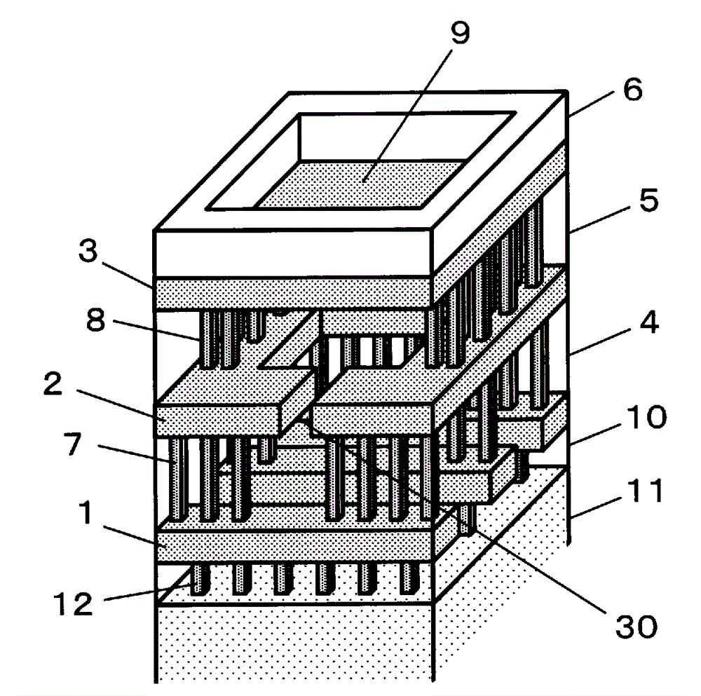
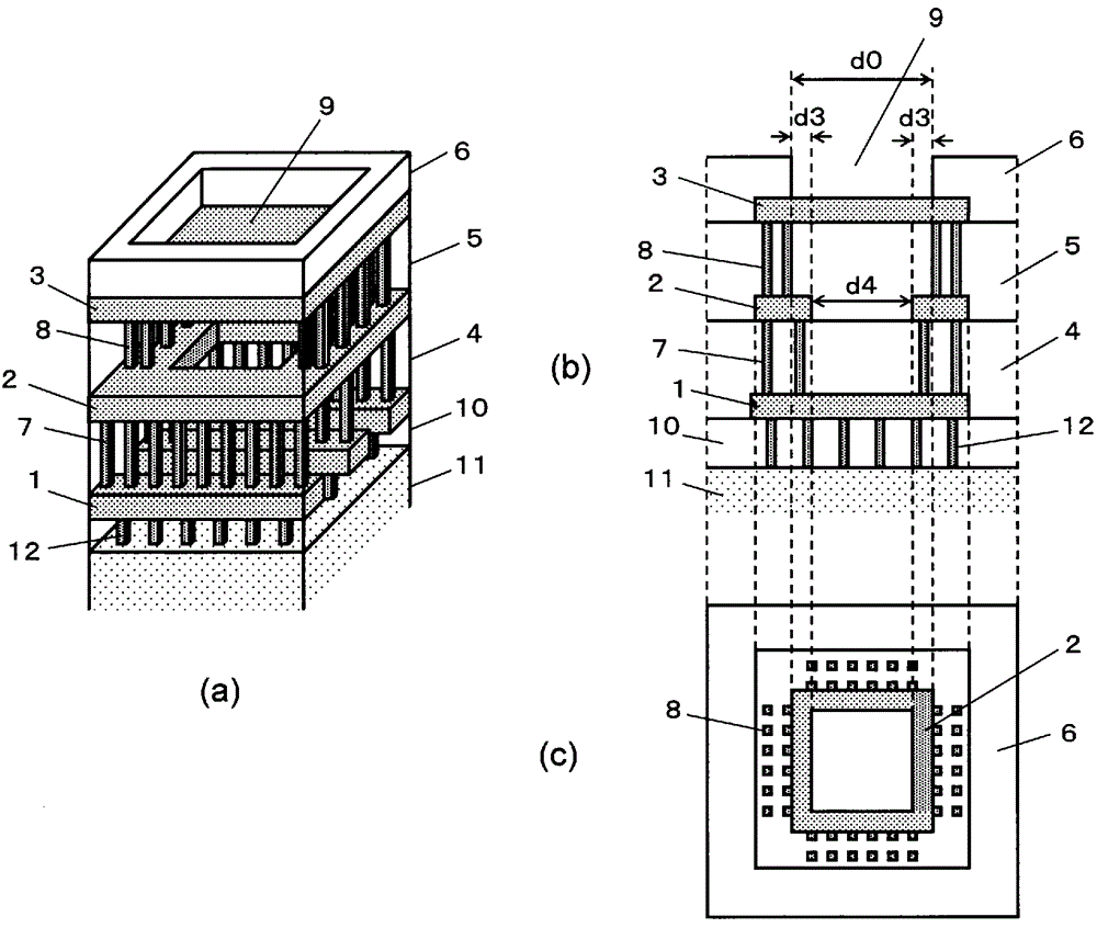
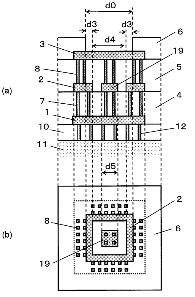
[0035] First, use figure 1 The pad structure of the semiconductor device of the present invention will be described. figure 1 (a) is a perspective view, (b) is a cross-sectional view, (c) is a plan view for explaining the relationship between the second metal film and the pad opening, and the uppermost metal film 3 is not shown.

[0036] Although not shown, elements are provided on the semiconductor substrate 11 . A first insulating film 10 is provided on a semiconductor substrate 11 , and a first metal film 1 is provided on the first insulating film 10 . The element and the first metal film 1 are electrically connected through the contact portion 12 . The second insulating film 4 is provided on the first metal film 1 , and the second metal film 2 is provided on the second insulating film 4 . The first metal film 1 and the second metal film 2 are electrically conn...


PUM


Abstract

In order to prevent chip size from being increased, while suppressing cracks below a pad opening, a protection film (6) has a pad opening (9) that exposes a part of a topmost layer metal film (3). The pad opening (9) is square, and the width of the opening is d0. A second metal film (2) has an opening below the pad opening (9). The opening is square, and the width of the opening is d4. The distance between the opening end of the protection film (6) and the opening end of the second metal film (2) is d3. The second metal film (2) has a rectangular ring shape, and protrudes to the inner side of the pad opening (9) by the distance d3.

Description

technical field [0001] The present invention relates to a semiconductor device having a pad structure. Background technique [0002] In order for the semiconductor device to exchange electrical signals with the outside, a wire bonding technique is used to connect pads of the semiconductor device and external connection terminals with metal wires. The wire bonding technique is a mechanical process of bonding a wire made of gold or the like to a pad of a semiconductor device using heat, ultrasonic waves, or a weight. Therefore, the semiconductor device may be damaged. use Figure 11 (a) and (b), explain this situation. The ballized wire 15 formed at the tip of the bonding wire 14 is crimped to the uppermost metal film 3 provided in the pad opening of the semiconductor device to form a crushed ball 16, and the bonding wire 14 is bonded to the uppermost layer of the pad opening. Metal film3. At this time, a crack 18 occurs in the insulating film 5 under the pad opening, which...

Claims


Application Information

Patent Timeline
Patent Type & Authority Applications(China)
IPC IPC(8): H01L21/60H01L21/3205H01L21/768H01L23/522
CPCH01L27/0296H01L2224/78301H01L2224/05096H01L2924/00014H01L24/05H01L2224/48463H01L24/85H01L2224/04042H01L2224/05014H01L2224/05085H01L24/78H01L2224/05095H01L2224/02166H01L2224/78303H01L2224/45144H01L23/522H01L2224/85181H01L2224/85205H01L2224/48451H01L2224/05011H01L2924/35H01L2224/05013H01L2224/05553H01L2224/05554H01L2224/05555H01L24/48H01L2224/05599H01L2224/05099H01L2924/00015H01L23/49827H01L23/5283H01L23/5226H01L23/60H01L24/45
Inventor 理崎智光中西章滋樱井仁美岛崎洸一
Owner SII SEMICONDUCTOR CORP
Why Eureka
Try Eureka