

Semiconductor integrated circuit
A technology of integrated circuits and semiconductors, applied in the manufacture of circuits, logic circuits, semiconductors/solid-state devices, etc.
- Summary
- Abstract
- Description
- Claims
- Application Information
AI Technical Summary
Problems solved by technology
Method used
Image

Examples
Embodiment 1
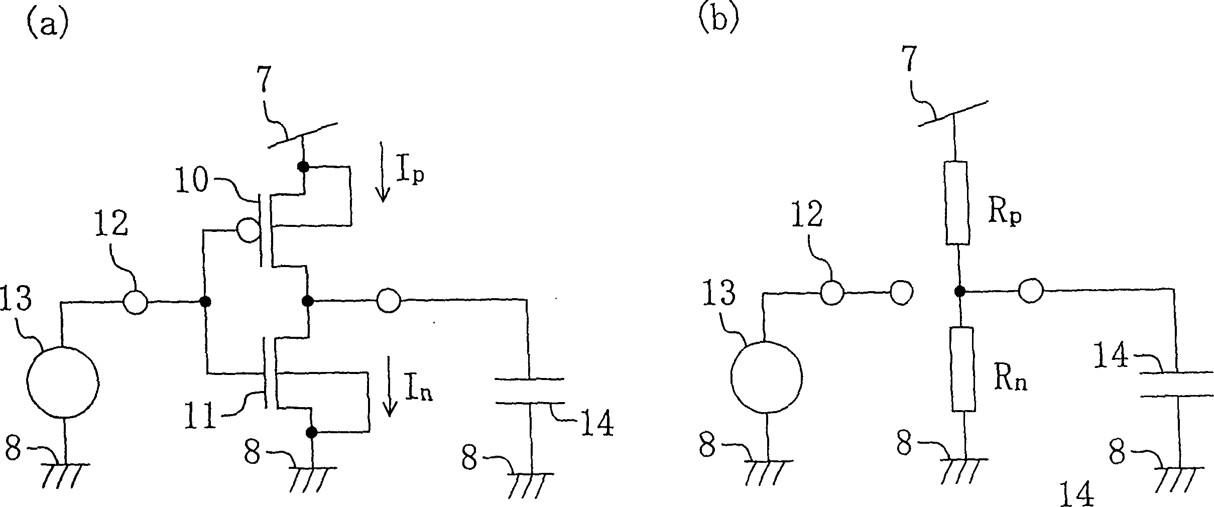
[0112] Figure 9 and Figure 10 Shows Example 1 of the present invention. Figure 9 (a) and (c) are configuration examples for an inverter circuit. The figure (a) is an inverter circuit in which PMOS 100 and NMOS 101 are connected in series, and the connection point of PMOS 100 and NMOS 101 is output terminal 102 .
[0113] In the inverter circuit, the source terminal of the PMOS 100 (first MOS transistor) 100 is connected to the terminal (power supply terminal) 18 of the power generator (conductance adjustment device and current adjustment device) 17, and the well terminal as the control terminal Connect to Terminal 19. In the operating state of the inverter circuit, both terminals 18, 19 are set to the first supply potential. In the non-operating state, the power supply potential of the terminal 18 is lowered to the second power supply potential Vdd2 (Vdd2<<Vdd1). At this time, if the input signal of the inverter circuit is the second power supply potential Vdd2 (H leve...
Embodiment 2
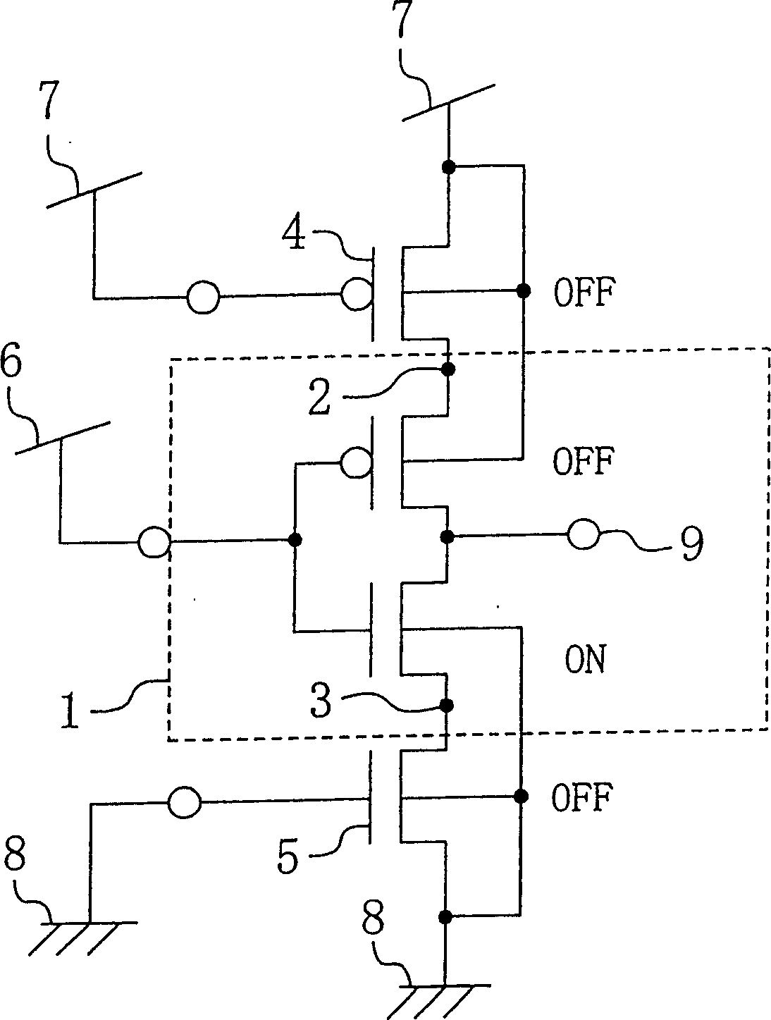
[0135] Next, Embodiment 2 of the present invention will be described. In this embodiment, the present invention is applied to SRAM. Although it is considered more difficult to apply the present invention to an SRAM than an inverter circuit, it is actually the same as an inverter circuit according to the characteristics of FIG. 7 .
[0136] Figure 11 is a structural diagram of the most widely used SRAM at present. The inverter circuit 17a (first signal processing circuit) is composed of a PMOS (first PMOS transistor) 100a and an NMOS (first NMOS transistor) 101a connected in series, and the connection point between the drain terminals thereof is an output terminal (the first output terminal). terminal) 102a, and the connection point between the gate terminals is an input terminal (first input terminal) 103a. In addition, the inverter circuit 18a (second signal processing circuit) is also composed of a PMOS (second PMOS transistor) 100b and an NMOS (second NMOS transistor) 101...
Embodiment 3
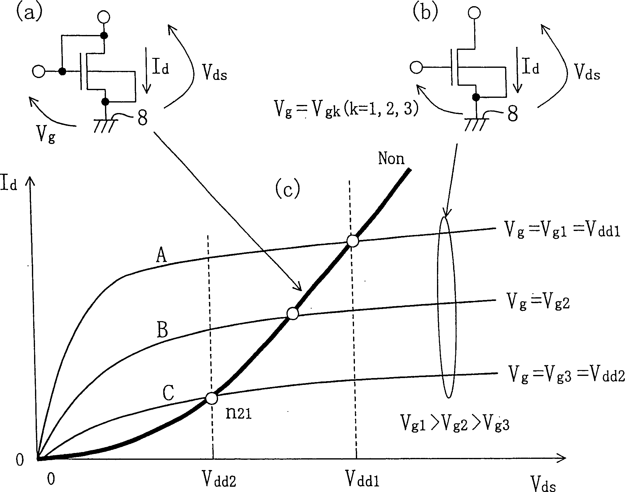
[0148] Next, Embodiment 3 of the present invention will be described. This embodiment is to apply the present invention to a NAND circuit. Such as Figure 16As shown, the structure of the 2-input NAND circuit is different from that of the inverter circuit in that the NMOSs 25 and 26 are connected in series or the PMOSs 27 and 28 are connected in parallel.
[0149] Logic circuits such as NAND circuits and NOR circuits including the inverter circuits discussed above are static circuits. In the case of a static logic circuit, the point that the output is determined by switching the PMOS and NMOS on and off is the same. For example, when the input terminals 29 and 30 are set at H level and H level, the output terminal 31 becomes L level. NMOS said Figure 5 The characteristics of Non in (b), but by making the characteristics of Non correspond to the case of replacing the series connection of NMOS25 and NMOS26 with one NMOS, and making the Poff characteristics of PMOS correspon...
PUM
 Abstract
Description
Claims
Application Information