Method and apparatus for accelerating processor to read and write scratch memory

A technology for accelerating processors and temporary registers. It is used in program control devices, electrical digital data processing, instruments, etc., and can solve problems such as poor read and write speed, poor performance of read and write registers, and large program capacity.

Inactive Publication Date: 2006-09-27
WINBOND ELECTRONICS CORP
View PDF0 Cites 0 Cited by
  • Summary
  • Abstract
  • Description
  • Claims
  • Application Information

AI Technical Summary

Problems solved by technology

[0004] However, the performance of the above-mentioned external ICE method in reading and writing the scratchpad is obviously not good, mainly because the internal data transfer instruction (MOV) used by the processor to read and write the internal scratchpad usually only needs one machine cycle (MACHINECYCLE). The external data transfer instruction (MOVX) used by the extended memory requires two machine cycles
And the MOVX data transmission instruction is executed. After the operation of the accumulator (ACC) is completed, it is written back (WRITE BACK) to the original scratchpad, which affects its read and write speed even more.
In addition, when reading and writing other temporary registers, the address (in Ri or DPTR) must also be advanced first, so its performance in reading and writing speed is extremely poor, and the required program capacity is also large
At the same time, it cannot meet many occasions with high requirements for reading and writing.
[0005] It can be seen from the above that when users use the SFR in the processor for various special functions, they must use ICE for debugging. However, the built-in ICE consumes a lot of resources, and the external ICE does not perform well in reading and writing. The Dilemma of Processor Development

Method used


Image

  • Method and apparatus for accelerating processor to read and write scratch memory
  • Method and apparatus for accelerating processor to read and write scratch memory
  • Method and apparatus for accelerating processor to read and write scratch memory

Examples


Embodiment Construction

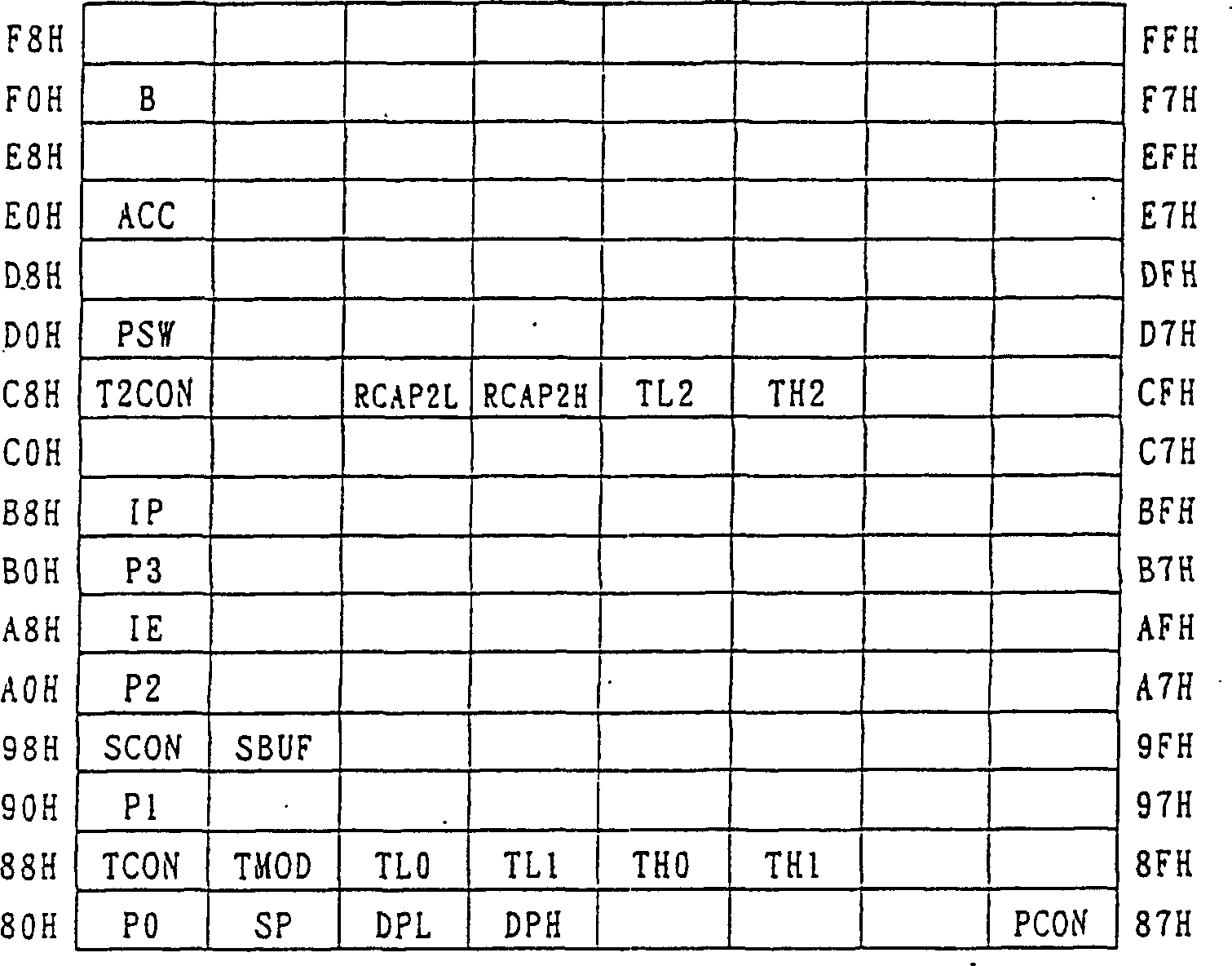
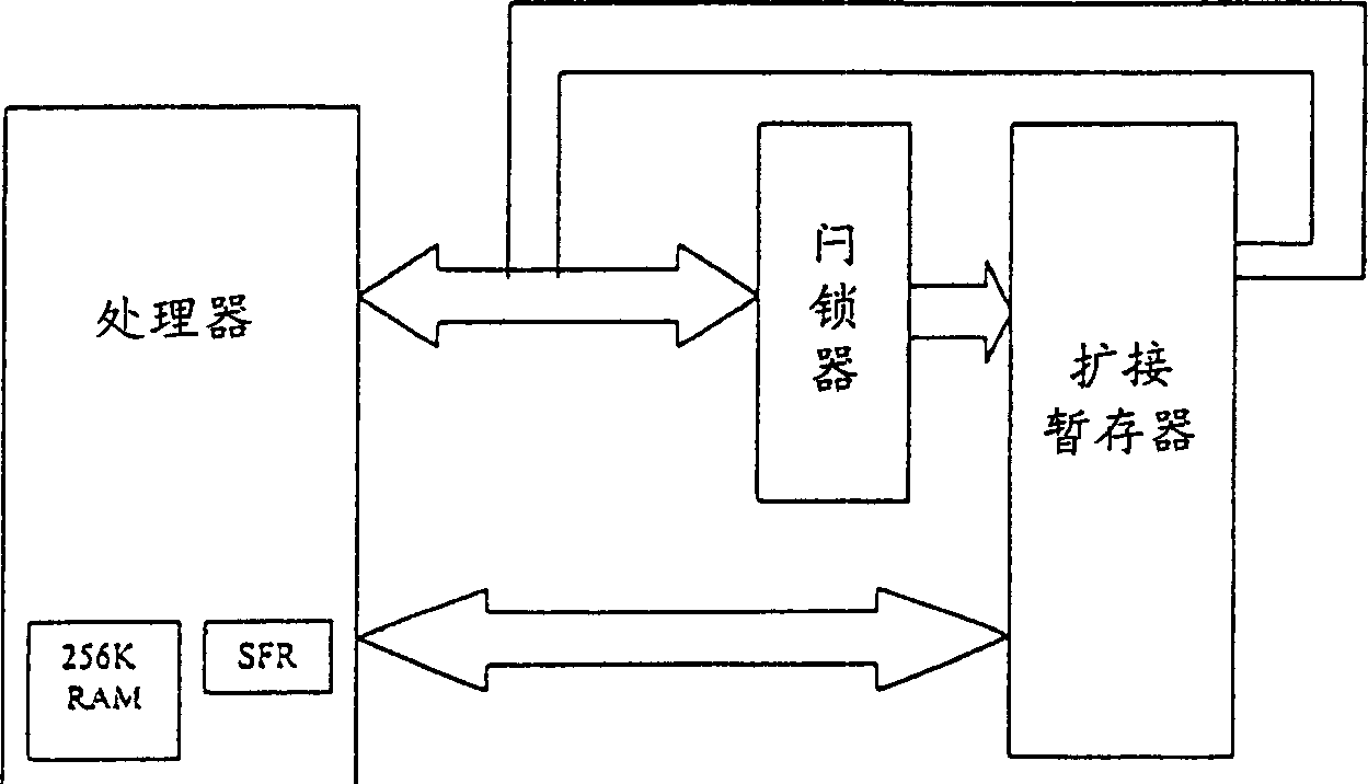
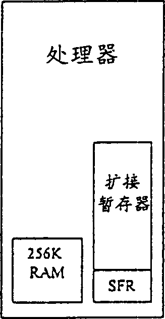
[0021] Firstly, in the present invention, the processor is externally connected with an expansion memory to establish an expansion temporary register. In this embodiment, an 8051 processor is used as an example. The extended register address is mapped to the idle address of the special function register (SFR) in the processor by means of memory mapping (MEMORY MAPPING).

[0022] The SFR is a 128-byte (Bytes) (80H~FFH) directly addressable memory area (see figure 1 As shown), in addition to the existing multiple groups of temporary registers, there are still many idle addresses, so the present invention maps the address of the extended temporary register to the idle address of SFR, so that in the normal operation mode, the The extended scratchpad is simulated as an internal scratchpad, and the extended scratchpad can be read and written by internal data transfer instructions. Compared with the way of reading and writing external scratchpads by external data transfer instruction...


PUM


Abstract

The invention relates to a method to accelerate processor to read / write register and its device, mainly using processor to externally connect up with an extended memory and adopting MEMORY MAPPING mode to map register address established in the extended memory with idle SFR address in the processor, and also using a sign switch processor as integrated computer emulation (ICE) mode or normal operating mode, and the processor still uses external data transmission instruction as in ICE mode and internal one as in normal operating mode to read / write external register, respectively.

Description

(1) Technical field [0001] The invention relates to a method and a device for a processor to read and write a temporary register, in particular to a method and a device for accelerating a processor to read and write a temporary register by using a memory mapping (MEMORY MAPPING) mode. (2) Background technology [0002] In the single chip of the 8051 series, the special function register (SFR) plays a very important role, which is a 128-byte (Bytes) directly addressable memory area. Its direct address is 80H~FFH, which is a temporary register used to store peripheral device control, status and data. Any use of interrupt, serial port, timer / counter and other functions must first be performed in the relevant control registers of SFR. set up. [0003] However, once the scratchpad in the SFR is used, in order to debug (debug) and other requirements during development, it is often necessary to build an online emulator (ICE, In-CircuitEmulator) in the processor for the aforementio...

Claims


Application Information

Patent Timeline
Patent Type & Authority Patents(China)
IPC IPC(8): G06F11/00G06F13/42G06F9/44
Inventor 陈志勇
Owner WINBOND ELECTRONICS CORP
Why Eureka
Try Eureka