
Plasma display device and method for controlling the same

A display device and plasma technology, applied to static indicators, instruments, etc., can solve problems such as damaged components and large output loss

Inactive Publication Date: 2007-08-15
HITACHI CONSUMER ELECTRONICS CORP
View PDF7 Cites 0 Cited by
  • Summary
  • Abstract
  • Description
  • Claims
  • Application Information

AI Technical Summary

Problems solved by technology

In this case, the output loss becomes large in the driving operation of the drive circuit, so that each of the elements constituting the drive circuit generates large heat, thereby causing damage to the elements in some cases

Method used


Image

  • Plasma display device and method for controlling the same
  • Plasma display device and method for controlling the same
  • Plasma display device and method for controlling the same

Examples


no. 1 example

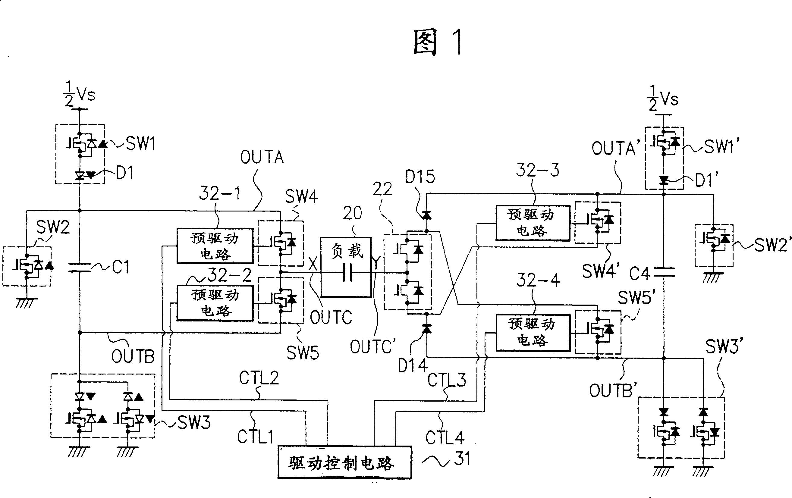
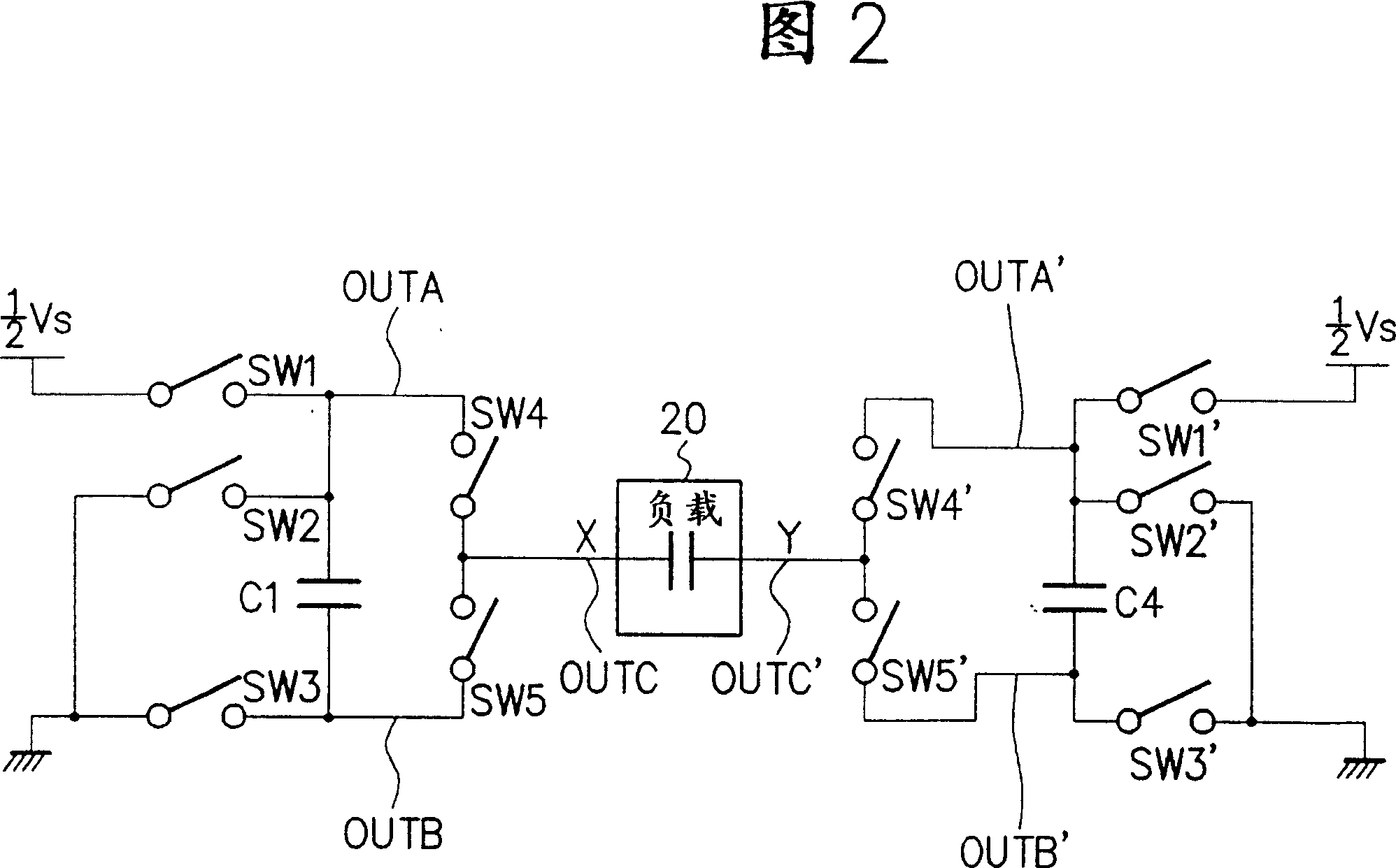
[0079] FIG. 1 is a circuit diagram showing the arrangement of a drive circuit for AC driving a PDP according to a first embodiment. Incidentally, the driving circuit shown in FIG. 1 according to this embodiment is applicable to an AC-driven PDP shown in FIGS. 17 and 18, which show its overall arrangement and structure of units constituting a pixel. It is to be understood that elements having the same number in Figures 1 and 19 have the same function.

[0080] Referring to FIG. 1, the load 20 is the total capacitance of cells formed between one common electrode X and one scan electrode Y. Referring to FIG. The common electrode X and the scan electrode Y are formed on the load 20 .

[0081] On the common electrode X side, switches SW2 and SW1 are connected in series between a power supply line for potential (Vs / 2) supplied from a power supply (not shown) and ground (GND). One terminal of capacitor C1 is connected to an interconnection node of two switches SW1 and SW2, and swit...

no. 2 example

[0152] Now, the present invention is explained with reference to the second embodiment.

[0153] Fig. 13 is a circuit diagram showing the arrangement of a drive circuit for AC driving the PDP according to the second embodiment. Incidentally, the driving circuit shown in FIG. 13 according to this embodiment is applicable to the AC-driven PDP device shown in FIGS. 17 and 18, which show its overall arrangement and the structure of a unit constituting a pixel. Incidentally, in FIG. 13, the same elements as those shown in FIG. 1 are given the same reference numerals, and explanations are not repeated.

[0154] The driving circuit according to the first embodiment is provided with a pre-driving circuit for each of the output elements. However, the drive circuit according to the second embodiment is provided with a pre-drive circuit on each side of the common electrode X and the scan electrode Y for switching and generating control for each of the output elements etc. in the pre-dri...


PUM


Abstract

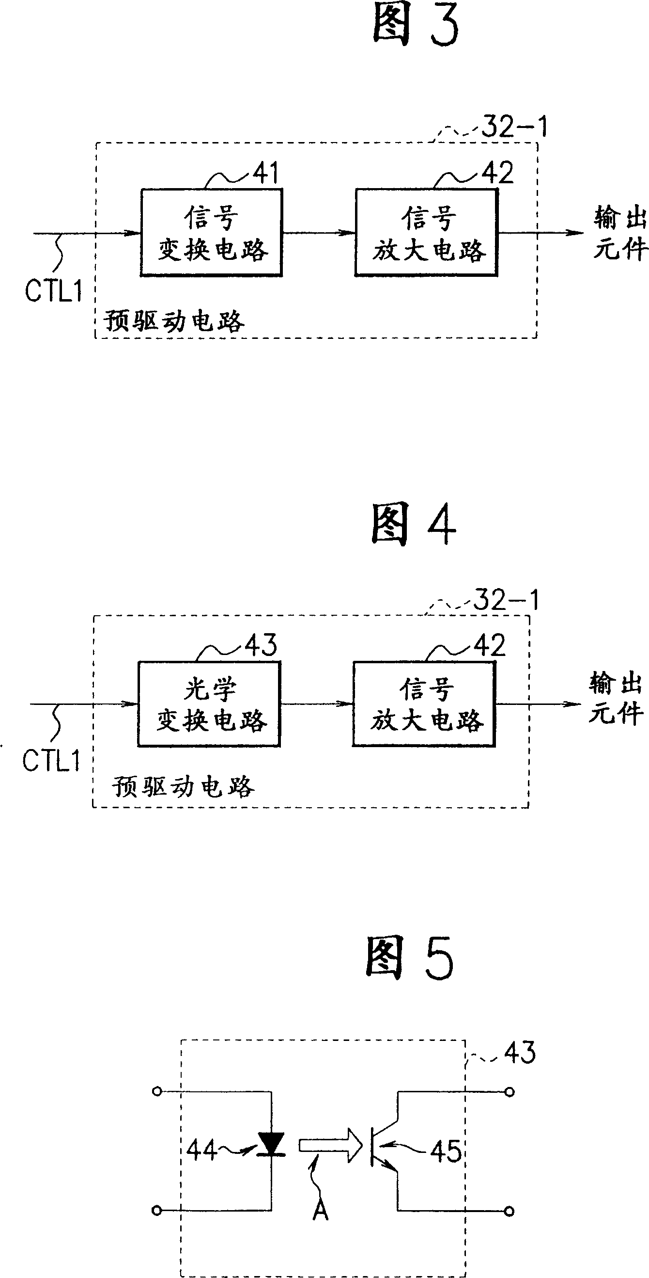
A signal transfer circuit (41) in a pre-drive circuit (32-1) converts the reference potential of a control signal, supplied from a drive control circuit, to the reference potential of an output element. The control signal is then amplified in a signal amplifier circuit (42) and thereafter supplied to the output element. This makes it possible to isolate the reference potential and transfer the control signal to the output element even when the reference potentials of the drive control circuit and the control signal are different from that of the output element. The drive control circuit can also be prevented from being affected by variations in potential of the output element or the like.

Description

[0001] The patent application of the present invention is a divisional application of the patent application for invention with the application number 01142463.X, the application date being November 29, 2001, and the invention name being "plasma display device and method for controlling it". technical field [0002] The present invention relates to a plasma display device and a method for controlling a plasma display device. More particularly, the present invention relates to a plasma display device and a method for controlling the plasma display device, preferably used in a driving circuit for driving each unit constituting a display portion and for controlling a driving circuit. The plasma display devices are driven by alternating currents with different reference potentials between the drive control circuits of the circuit. Background technique [0003] Conventionally, an AC-driven plasma display panel (PDP), one of flat display panels, is classified into a two-electrode ...

Claims


Application Information

Patent Timeline
Patent Type & Authority Patents(China)
IPC IPC(8): G09G3/28G09G3/20G09G3/288G09G3/291G09G3/296G09G3/298
CPCG09G2320/046G09G3/296G09G2310/066G09G3/2965
Inventor 小野泽诚岸智胜富尾重寿坂本哲也
Owner HITACHI CONSUMER ELECTRONICS CORP
Learn More