Plasma display device and method for controlling the same
A display device and plasma technology, applied to static indicators, instruments, etc., can solve problems such as damaged components and large output loss
- Summary
- Abstract
- Description
- Claims
- Application Information
AI Technical Summary
Problems solved by technology
Method used
Image
Examples
no. 1 example
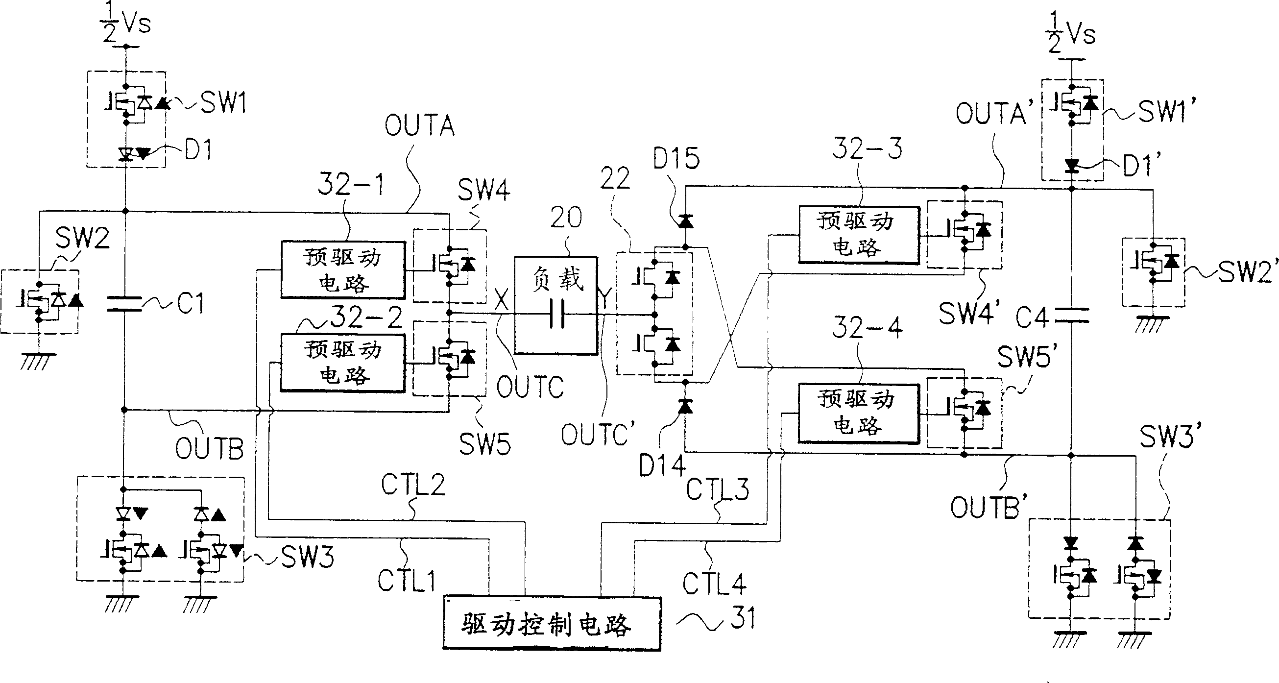
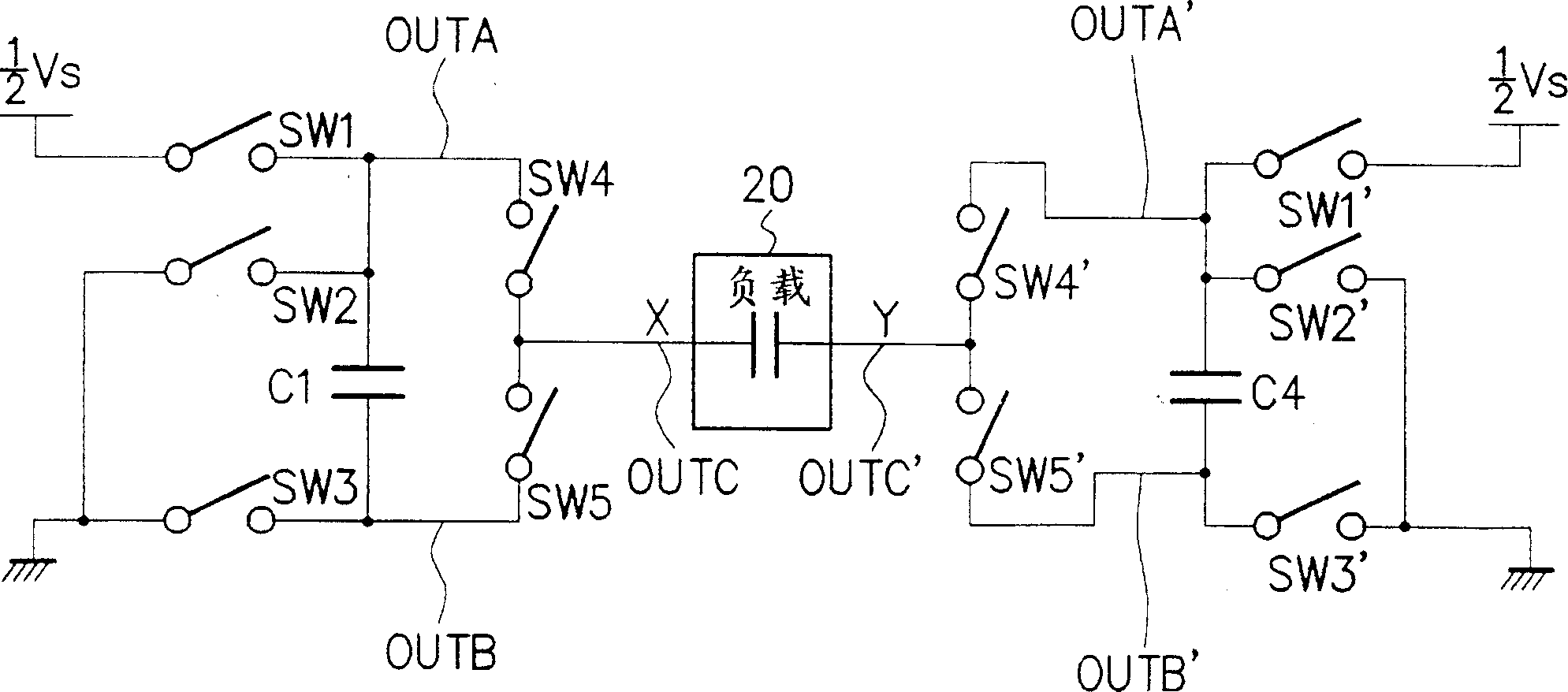
[0079] figure 1 is a circuit diagram showing the arrangement of a drive circuit for AC driving the PDP according to the first embodiment. Incidentally, according to this embodiment expressed in figure 1 The drive circuit in can be applied to Figure 17 The AC-driven PDP shown in and 18 shows its overall arrangement and the structure of a unit constituting a pixel. to understand in figure 1 and 19 Components with the same reference number have the same function.
[0080] refer to figure 1 , the load 20 is the total capacitance of the cells formed between one common electrode X and one scan electrode Y. The common electrode X and the scan electrode Y are formed on the load 20 .
[0081] On the common electrode X side, switches SW2 and SW1 are connected in series between a power supply line for potential (Vs / 2) supplied from a power supply (not shown) and ground (GND). One terminal of capacitor C1 is connected to an interconnection node of two switches SW1 and SW2, and...
no. 2 example
[0152] Now, the present invention is explained with reference to the second embodiment.
[0153] Fig. 13 is a circuit diagram showing the arrangement of a drive circuit for AC driving the PDP according to the second embodiment. Incidentally, the driving circuit shown in FIG. 13 according to this embodiment can be applied to Figure 17 and the AC-driven PDP device shown in 18, which shows its overall arrangement and the structure of a unit constituting a pixel. Incidentally, in Figure 13, with figure 1 The same elements as those shown in are given the same reference numerals, and explanations are not repeated.
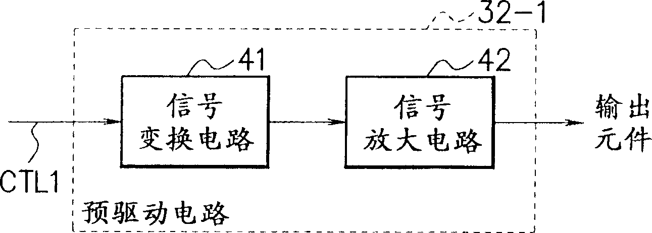
[0154] The driving circuit according to the first embodiment is provided with a pre-driving circuit for each of the output elements. However, the drive circuit according to the second embodiment is provided with a pre-drive circuit on each side of the common electrode X and the scan electrode Y for switching and generating control for each of the output elements etc....
PUM
 Abstract
Description
Claims
Application Information


