Integrated optical switch array

An optical switch and array technology, applied in optics, light guides, optical components, etc., can solve the problems of low switch packaging efficiency and non-unique optical path

Inactive Publication Date: 2002-05-08
LYNX PHOTONIC NETWORKS
View PDF2 Cites 9 Cited by
  • Summary
  • Abstract
  • Description
  • Claims
  • Application Information

AI Technical Summary

Problems solved by technology

[0009] 2. In general, the optical path from a specific input waveguide to a specific output waveguide through the crossbar arra

Method used


Image

  • Integrated optical switch array
  • Integrated optical switch array
  • Integrated optical switch array

Examples


Embodiment Construction

[0034] The geometry of the integrated optical switch array of the present invention allows it to be manufactured more compactly than known optical switch arrays.

[0035] The working principle of the optical switch array of the present invention can be fully understood with reference to the drawings and descriptions thereof.

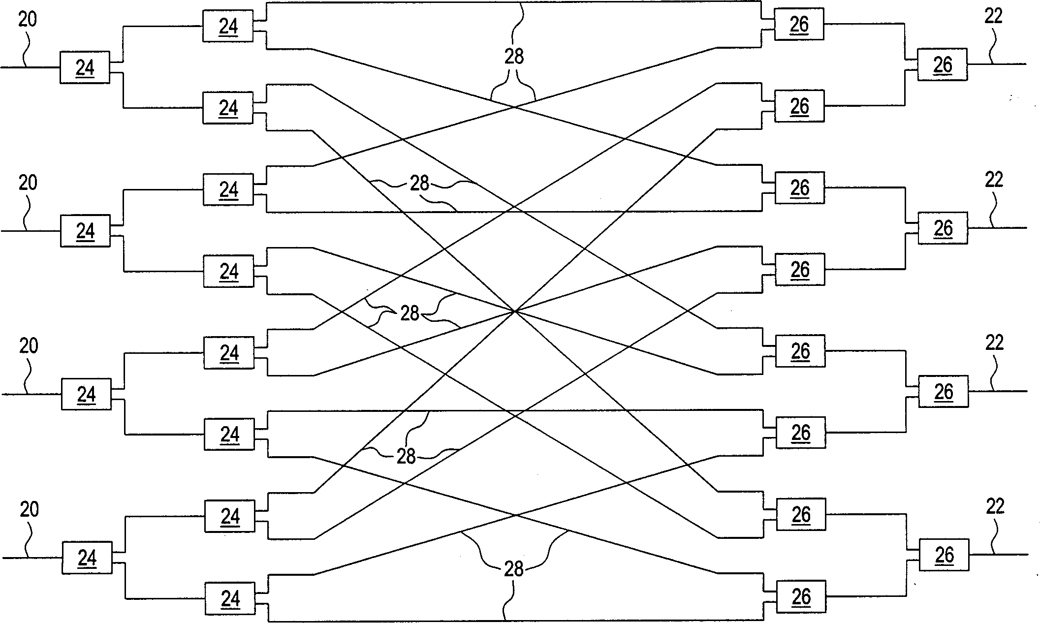
[0036] Referring now to the drawings, FIG. 5A is a schematic diagram of a switch array of the present invention for coupling input waveguides 140a, 140b, 140c and 140d to output waveguides 142a, 142b, 142c and 142d. Input waveguide 140a, coupled to output waveguide 142a with 1x2 switch 144aa through intermediate waveguide 148aa and passive y-tangle combiner 146aa, coupled to output waveguide 142a with 1x2 switch 144ab through intermediate waveguide 148ab and passive y-tap combiner 146ab to Output waveguide 142b, coupled to output waveguide 142c with 1x2 switch 144ac via intermediate waveguide 148ac and passive y-junction combiner 146ac, and coupled to O...


PUM


Abstract

An optical switch array is provided in which at least three input waveguides are coupled to at least three output waveguides. Each of the input waveguides is coupled in the same order to each of the output waveguides by a coupling element such as a y-junction combiner, via an intermediate waveguide and a switching mechanism that includes a coupling element such as a 1 x 2 switch. For compactness, the coupling elements that couple to the same input waveguide are mutually displaced along the output waveguides.

Description

technical field [0001] The present invention relates to optical switch arrays, and more particularly to optical switch arrays of extremely small geometries in which random combinations of inputs and outputs are unambiguously addressable. Background technique [0002] Integrated optical switches are well-known technologies. For a review of the early state of the art, see Lars Thylen's "Integrated Optics in LiNbO3: recent developments in devices for telecommunications" Journal of Lightwave technology vol.6 no.6 (June 1988), pp 847-861 . The waveguide is fabricated on the substrate by locally processing the lithium niobate substrate to increase the refractive index. For example, the refractive index of lithium niobate can be locally increased by diffusing titanium into the substrate. To transfer light from one waveguide into another, they can be coupled by local optoelectronic control of their refractive index. Well-known examples of optoelectronic switches include direction...

Claims


Application Information

Patent Timeline
IPC IPC(8): G02F1/313G02B6/12G02B6/35G02B26/00G02F1/035H04Q3/52H04Q11/00
CPCH04Q2011/0052G02B2006/12145H04Q2011/0041H04Q2011/0058H04Q2011/0015H04Q2011/0047G02B2006/12147H04Q11/0005G02B26/00
Inventor 戴维·尼尔
Owner LYNX PHOTONIC NETWORKS
Why Eureka
Try Eureka