Conductor pattern formed by magnetic force

A conductor pattern, magnetization pattern technology, applied in semiconductor devices, semiconductor/solid-state device manufacturing, chemical/electrolytic methods to remove conductive materials, etc., can solve problems such as rising costs

Inactive Publication Date: 2002-12-04
HEWLETT PACKARD CO
View PDF0 Cites 5 Cited by
  • Summary
  • Abstract
  • Description
  • Claims
  • Application Information

AI Technical Summary

Problems solved by technology

Unfortunately, the cost of lithography generally rises with

Method used


Image

  • Conductor pattern formed by magnetic force
  • Conductor pattern formed by magnetic force
  • Conductor pattern formed by magnetic force

Examples


Embodiment Construction

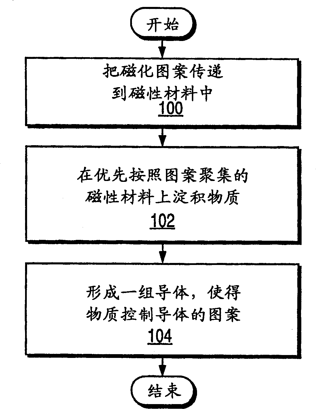
[0014] figure 1 A method of forming a conductor pattern using magnetic force according to the present technology will be described by way of example.

[0015] At step 100 a magnetization pattern is transferred into a magnetic material. In one embodiment, in step 100 said pattern is transferred into said magnetic material provided on a magnetic tape.

[0016] The pattern passed in step 100 can be any pattern. The pattern can be tailored to the specific use of the conductor. Various examples of uses include conductors associated with memory bit lines and / or word lines.

[0017] In step 102 , a substance preferentially assembled, ie aggregated, according to the pattern delivered in step 100 is deposited on the magnetic material. This substance protects the regions of magnetic material in a pattern corresponding to the desired pattern of the conductor to be formed.

[0018] At step 104, a set of conductors is formed such that the substance controls the pattern of the conducto...


PUM


Abstract

A method of forming a conductor pattern using magnetic force is disclosed. The method includes: transferring a magnetization pattern into a magnetic material; and depositing a species on the magnetic material, the species preferentially accumulating according to the pattern in the magnetic material. A set of conductors is then formed such that the substance controls the pattern of the conductors.

Description

technical field [0001] This invention relates to the field of forming conductors. More specifically, the present invention relates to forming conductor patterns using magnetic force. Background technique [0002] A typical integrated circuit includes a set of conductors arranged in a pattern according to the required electrical interconnections within the integrated circuit. For example, memories typically include a set of top conductors and a set of bottom conductors, each arranged in a pattern, the latter providing access to the memory cells. [0003] Conductors in integrated circuits are typically formed on silicon substrates using photolithographic techniques. Similar photolithographic techniques are typically used to form conductors on flexible substrates such as plastics. Unfortunately, the cost of photolithography generally rises with the density of circuit elements that include the conductors. It would be desirable to provide an alternative method of forming cond...

Claims


Application Information

Patent Timeline
IPC IPC(8): H01L21/288C23F1/02C23F4/00G11B5/84H05K3/06
CPCC23F1/02C23F4/00H05K3/065H01L2224/11G11B5/84
Inventor R·H·亨泽
Owner HEWLETT PACKARD CO
Why Eureka
Try Eureka