Display device and electronic machine

A technology for display devices and display areas, which is applied in the direction of electric solid devices, static indicators, instruments, etc., and can solve the problems of reducing the utilization efficiency of display areas, difficult to display areas, and inability to use substrates, etc.

Inactive Publication Date: 2003-09-03
ELEMENT CAPITAL COMMERCIAL CO PTE LTD
View PDF0 Cites 8 Cited by
  • Summary
  • Abstract
  • Description
  • Claims
  • Application Information

AI Technical Summary

Problems solved by technology

In such a display device, there is a problem that the drive circuit and / or control circuit must be arranged on the substrate, which increases the size of the substrate, or the area where these circuits are arranged is difficult to use as a display area, so it cannot be used. Effective use of the substrate as a display area
In addition, not only the connection wires from the designated power supply to the above-mentioned drive circuit and / or control circuit must also be arranged on the substrate, but also the connection wires from the control circuit to the drive circuit must also be arranged on the substrate, thus further reducing the display area. utilization efficiency

Method used


Image

  • Display device and electronic machine
  • Display device and electronic machine
  • Display device and electronic machine

Examples


Embodiment Construction

[0031] Preferred embodiments of the present invention are described below with reference to the accompanying drawings. The embodiments concerned are merely one form of the present invention, and do not limit the present invention, and can be modified arbitrarily within the scope of the technical idea of ​​the present invention. In addition, in each of the following figures, in order to make each layer and each member clearly identifiable on the drawing, each layer and each member have a different scale.

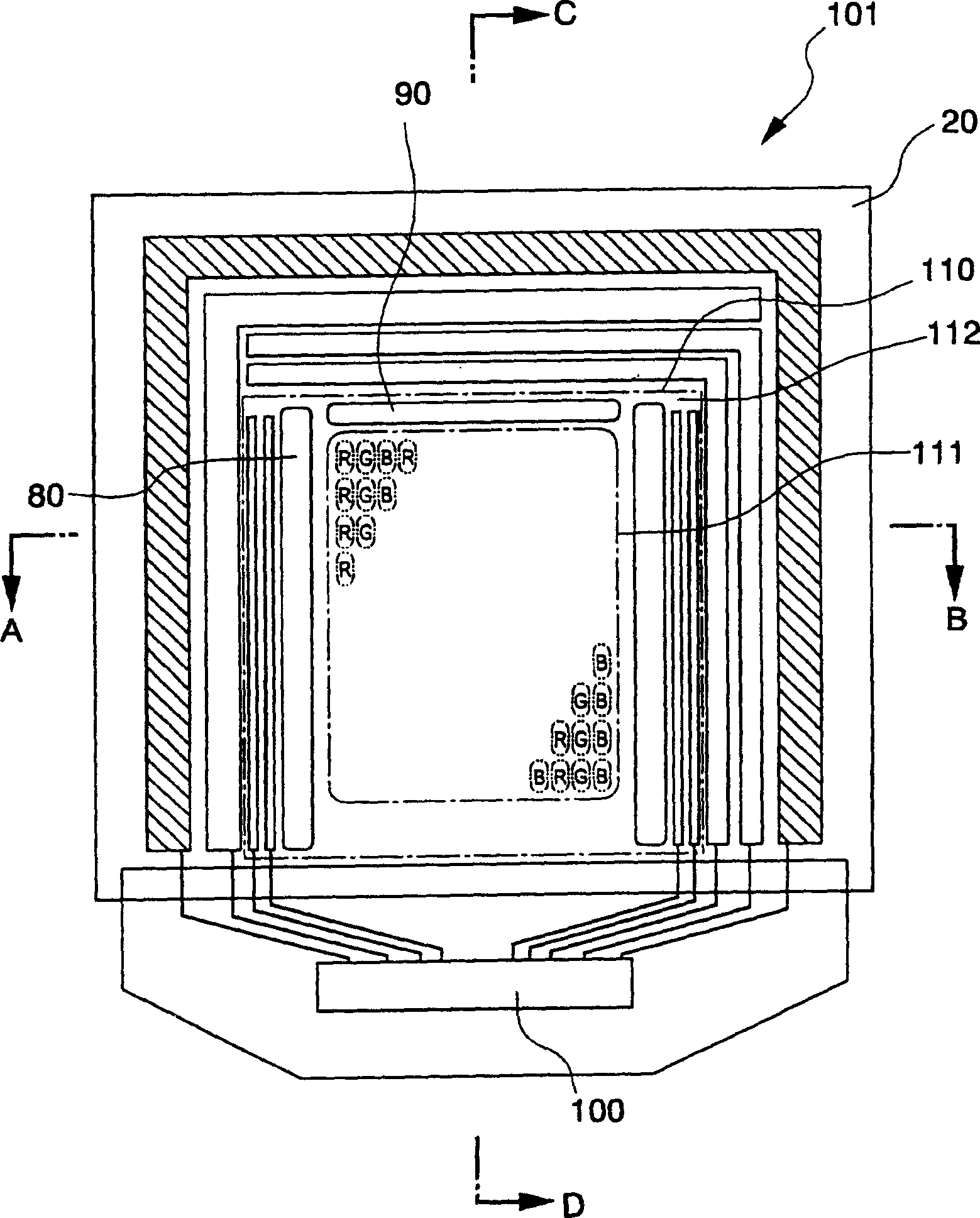
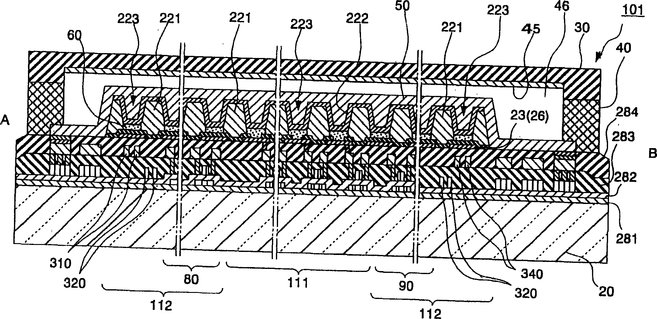
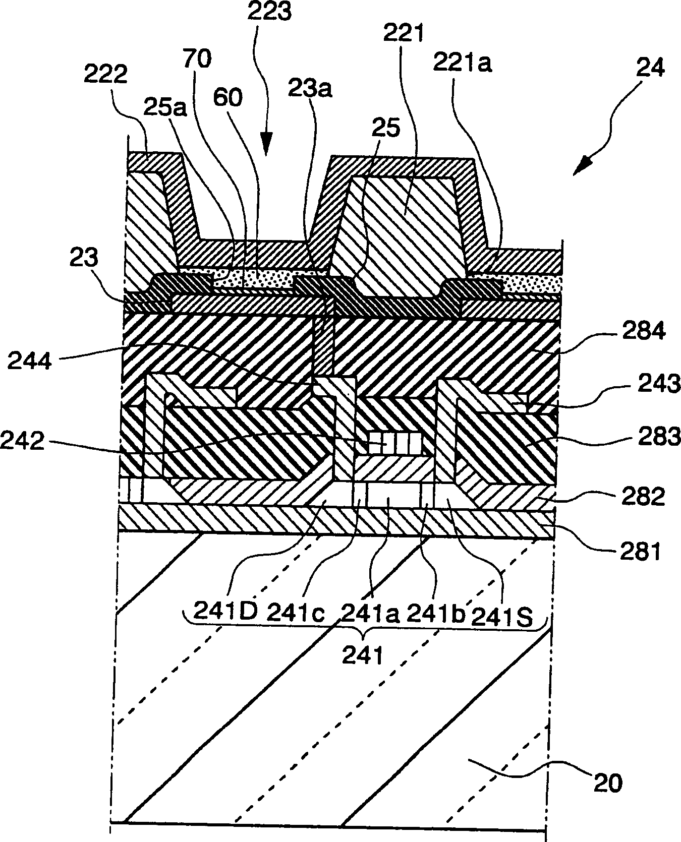
[0032] First, an embodiment in which the configuration of the present invention is applied to an EL display device using electroluminescence (hereinafter referred to as EL) as an example of an electro-optical substance constituting a display main layer will be described. figure 1 as well as figure 2 A schematic plan view and an A-B cross-sectional view of the configuration of the EL display device according to this embodiment are shown. The EL display device 101 shown in t...


PUM

PropertyMeasurementUnit
thicknessaaaaaaaaaa
thicknessaaaaaaaaaa
thicknessaaaaaaaaaa

Abstract

The patent relates to a display device and a electric device. A bank layer 221 and a recessed compartment area 223 compartmentalized by the bank layer 221 are arranged in a predetermined matrix pattern on the substrate 20. A real pixel part 111 for display and a dummy pixel part 112 not for display are formed in a pixel part to be a display part. A scanning line driving circuit 80 for controlling the output of scanning signals that pass through scanning lines and a drive controlling signal conducting part 320 through which drive control signals pass to drive the scanning line driving circuit 80 are also provided on the substrate 20. In the plan view of the substrate 20, the drive controlling signal conducting part 320 is superimposed at least partly on the recessed compartment area 223 of the dummy pixel part 112. Thereby, the display and electronic instrument can effectively utilize a substrate surface, and prevent or suppress a external effect on a drive controlling signal.

Description

technical field [0001] The present invention relates to a display device and its electronic equipment. Background technique [0002] Conventionally, optical display devices such as liquid crystal display devices and EL display devices have a structure in which a plurality of circuit elements, electrodes, liquid crystal or EL elements, etc. are stacked on a substrate. For example, in an EL display device, a light-emitting layer including a light-emitting substance is sandwiched between an anode and a cathode electrode layer, and the holes injected from the anode side and the electrons injected from the cathode side are used to create a fluorescent energy. A phenomenon in which light is emitted when the light-emitting layer is recombined and loses momentum from the excited state. [0003] As a driving method of such an EL display device, it is known that scanning lines in the row direction and data lines in the column direction are arranged in a matrix, and at the same time, ...

Claims


Application Information

Patent Timeline
Patent Type & Authority Applications(China)
IPC IPC(8): G09G3/30G02F1/1362H01L27/32
CPCH01L27/3276H01L27/3246H01L27/3223G02F1/13454H10K59/88H10K59/122H10K59/131G09G3/30
Inventor 中西早人
Owner ELEMENT CAPITAL COMMERCIAL CO PTE LTD
Why Eureka
Try Eureka