Storage circuit with redundant structure

A memory circuit and redundant memory technology, applied in the field of memory circuits, can solve problems such as selection start timing delay and the like

Inactive Publication Date: 2004-05-05
FUJITSU LTD
View PDF1 Cites 8 Cited by
  • Summary
  • Abstract
  • Description
  • Claims
  • Application Information

AI Technical Summary

Problems solved by technology

Therefore, the selection start timing on the spare sector side is delayed due to the time required for comparison and judgment of redundant addresses.

Method used


Image

  • Storage circuit with redundant structure
  • Storage circuit with redundant structure
  • Storage circuit with redundant structure

Examples


no. 2 example

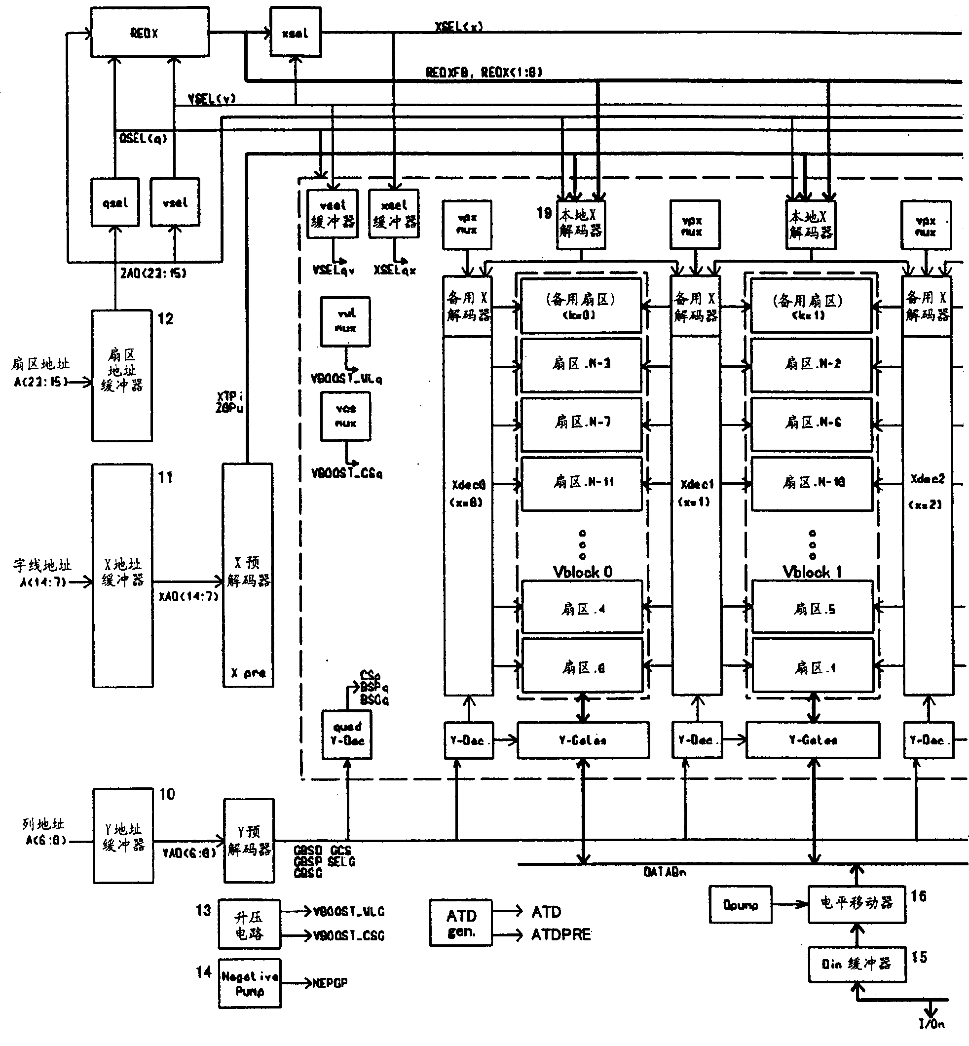
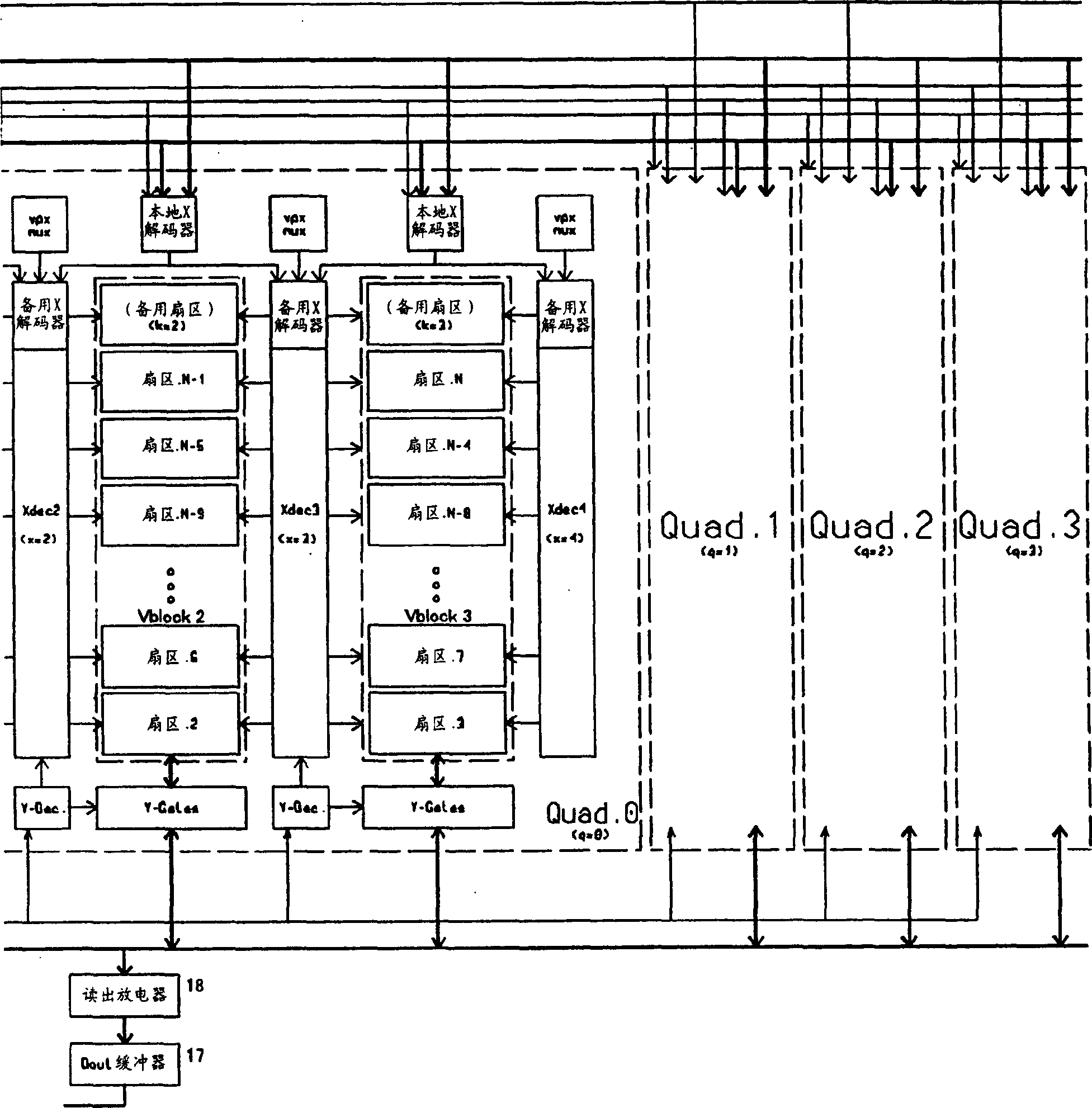
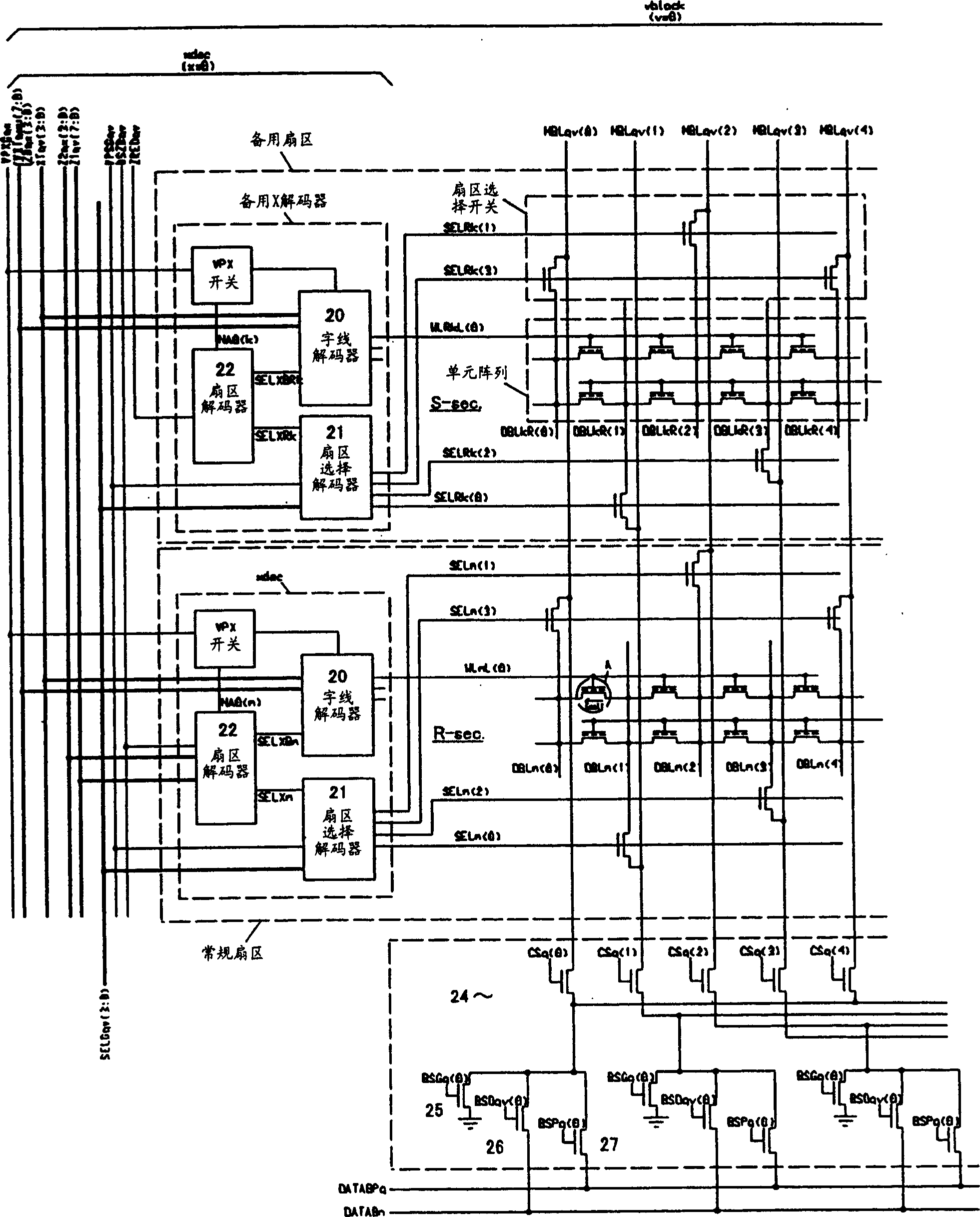
[0100] Next, a second embodiment will be described. The memory circuit of this embodiment also includes a plurality of conventional sectors and spare sectors, as shown in Figures 1, 2 and 3, and further includes a redundancy judgment circuit REDX, as Figure 9 shown in . In response to the test signal TEST (first signal), the redundancy judgment circuit REDX sets the redundancy judgment signal REDXFB to a matching state and enables access to the spare sector regardless of the address in the redundancy memory. For this purpose, AND gates 34, 36 and 38 are provided. Therefore, the other determination signals REDX ( 0 ), ( 1 ) are also forced to be in the matching state, and the simultaneous erase mode disable signal DISFCERB is also forcibly in the matching state (disabled state).

[0101] In addition, in response to the redundancy disable signal DISRED (second signal), the redundancy judgment circuit REDX sets the redundancy judgment signal REDXFB to a mismatch state regardle...


PUM


Abstract

A memory circuit has a plurality of blocks which further comprises a plurality of regular sectors and a spare sector, wherein each sector further comprises a plurality of memory cells, and when a regular sector in a first block is defective, this defective regular sector is replaced with a spare sector in a second block. And responding to an address to be supplied, the regular sector corresponding to the supplied address in the first block and the spare selector in the second block are selected simultaneously during a first period, and after the first period, selection of one of the regular sector and the spare sector is maintained according to the result of redundancy judgment on whether the supply address matches with the redundant address. Regardless the result of redundancy judgment on whether the supplied address matches the redundant address indicating the defective sector, a regular sector in the first block and the spare sector in the second block, to be a pair thereof, are set to selected status simultaneously during the first period when access operation stars, so a drop in access speed due to a redundancy judgment operation can be suppressed.

Description

technical field [0001] The present invention relates to a memory circuit having a redundant structure, and more particularly to a memory circuit in which a reduction in access speed due to redundant judgment is avoided. Background technique [0002] A semiconductor memory device has a redundant structure for repairing defective cells due to miniaturization due to capacity increase and other reasons. Various redundancy structures are used for semiconductor memories such as DRAM, SRAM, FeRAM, and EEPROM (flash memory). Among these memories, flash memory employs a redundant structure of bit lines as a repair method for defective cells. In other words, the bit line in the redundant cell side is used for reading instead of the bit line to which the defective cell belongs. This memory is described in Japanese Patent Application Laid-Open No. 2000-231795 (published on Aug. 22, 2000). [0003] In such a flash memory, due to an increase in capacity, defects in word lines and secto...

Claims


Application Information

Patent Timeline
Patent Type & Authority Applications(China)
IPC IPC(8): G11C16/06G11C16/02G11C29/00G11C29/04G11C29/24
CPCG11C29/82G11C29/24G11C29/846G11C29/00
Inventor 槻馆美弘栗原和弘笠靖中井努张雅迪
Owner FUJITSU LTD
Why Eureka
Try Eureka