

Circuit and method for supplying page mode operation in semiconductor storing device
A mode and page technology, applied in the field of circuits and methods providing page mode operation in semiconductor storage devices
- Summary
- Abstract
- Description
- Claims
- Application Information
AI Technical Summary
Problems solved by technology
Method used
Image

Examples
Embodiment Construction
[0036] The present invention is a semiconductor memory device that provides efficient page operation in a partially active mode of operation. Specifically, the circuits and methods of the preferred embodiments of the present invention are based on addressing schemes and control circuits that provide improved page mode operation and increased data access speeds for semiconductor memory devices with partially active architectures (eg, DRAM, FCRAM).
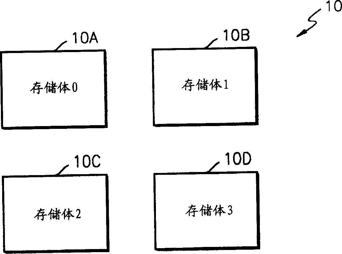
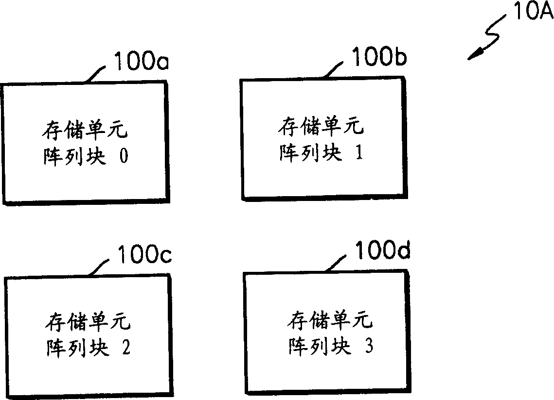
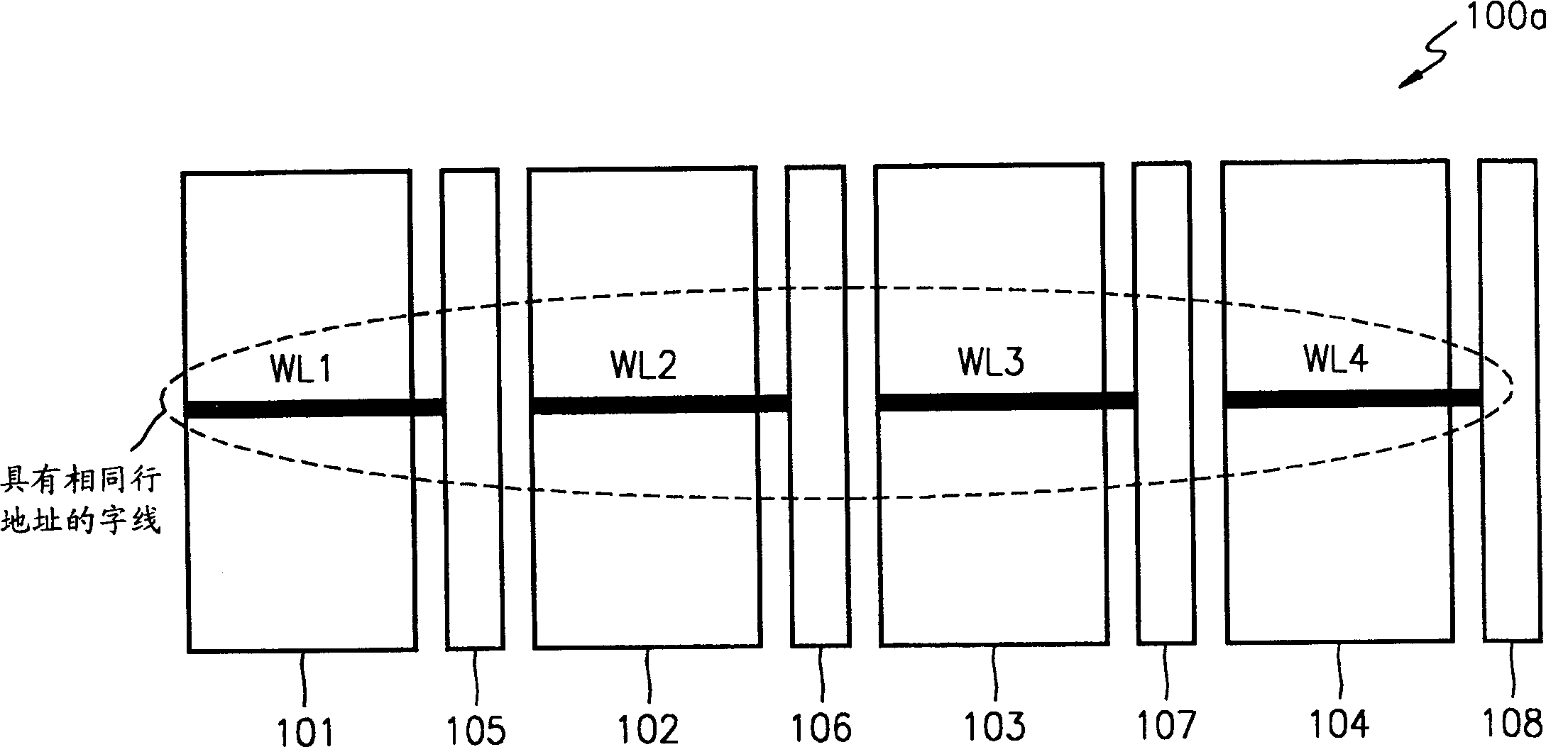
[0037] image 3 is a block diagram illustrating a semiconductor memory device having a partially active architecture according to an embodiment of the present invention, providing efficient page mode operation in a partially active mode of operation. see image 3 , a semiconductor memory device comprising: a memory cell array (100); a plurality of peripheral circuits (110 to 196) for inputting / outputting data to / from the memory cell array (100); a row address comparator (200); a command shifter ( 300). For purposes of illustratio...
PUM
 Abstract
Description
Claims
Application Information