Multi-layer insulation system for electrical conductors
A multi-layer insulation, electrical conductor technology, applied in the direction of conductor/cable insulation, conductors, insulators, etc.
- Summary
- Abstract
- Description
- Claims
- Application Information
AI Technical Summary
Problems solved by technology
Method used
Image
Examples
Embodiment 1A to 1E
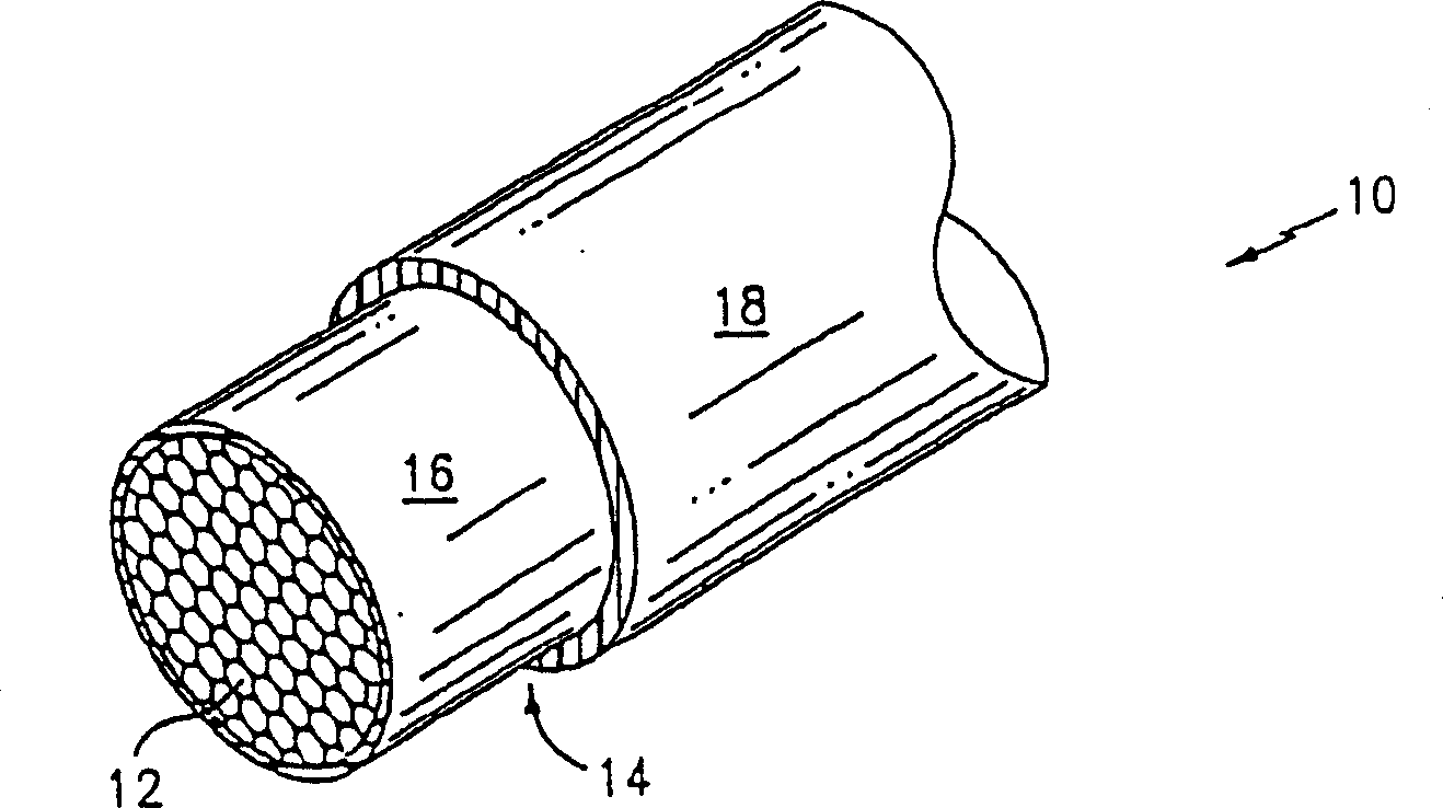
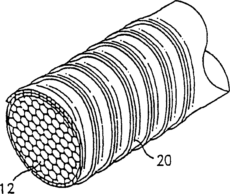
[0148] A continuous strip of polyimide film I having a width of 0.64 cm and a thickness of 0.03 mm was helically wound around the conductor at an overlap rate of 53%. The helically wound conductor is then heated in a continuous process to a temperature in excess of 300° C. for about 5 seconds to heat seal the overlapping portion of the polyimide film I strip, which is then cooled. The heat-sealed, spiral-wound polyimide film I inner layer has a thickness of 0.05 mm.
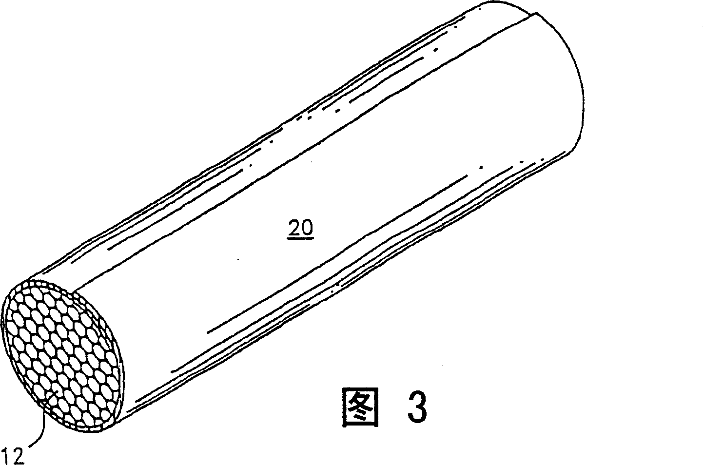
[0149] A certain amount of ETFE was mixed with 8wt% TAIC and 2wt% TiO 2 Mixing, and then using a single-screw extruder to extrude it to cover the inner layer of polyimide film I. This single-screw extruder has four heating zones, and the temperature in each zone is set at 200°C, 240°C, 275°C and 290°C. The thickness of the extruded ETFE layer was 0.13 mm.
[0150] The test sample is then irradiated with electron beam radiation and cooled with air. The total electron beam dosage was 10, 15, 20 or 30 Mrads, and...
Embodiment 2、3A to 3C、4
[0152] Examples 2, 3A to 3C, 4A and 4B
[0153] In addition to using different polyimide films to prepare test samples for each example, four wire structure test samples labeled Example 2, ten examples were prepared basically according to the same method as in Example 1 above. 3 test samples and six test samples of Example 4. As mentioned above, the total electron beam dosage was 10, 15, 20 or 30 Mrads, and the applied voltage was 120KV, 150KV or 0.5MEV.
[0154] The wire constructions tested are more fully described in Table 1 below.
Embodiment 5
[0156] The one thousand foot long wire construction labeled Example 5 was prepared essentially in the same manner as in Examples 1A to 1E above, except that the total electron beam dose was 18 Mrads and the applied voltage was 0.5 MeV.
[0157] The wire constructions tested are more fully described in Table 1 below.
PUM
| Property | Measurement | Unit |
|---|---|---|
| width | aaaaa | aaaaa |
| thickness | aaaaa | aaaaa |
| thickness | aaaaa | aaaaa |
Abstract
Description
Claims
Application Information


