Method for the manufactur of a printed circuit and planar antenna manufactured with this printed circuit

A technology of printed circuit and planar antenna, applied in the direction of printed circuit manufacturing, printed circuit, printed circuit, etc., can solve problems such as substrate limitation, and achieve the effect of high conductivity, low resistance, and saving raw materials

Inactive Publication Date: 2004-09-08
MICROCONNECTIONS
View PDF3 Cites 8 Cited by
  • Summary
  • Abstract
  • Description
  • Claims
  • Application Information

AI Technical Summary

Problems solved by technology

Therefore, this method has the disadvantage that the substrates that can be used are limited

Method used


Image

  • Method for the manufactur of a printed circuit and planar antenna manufactured with this printed circuit
  • Method for the manufactur of a printed circuit and planar antenna manufactured with this printed circuit
  • Method for the manufactur of a printed circuit and planar antenna manufactured with this printed circuit

Examples


Embodiment Construction

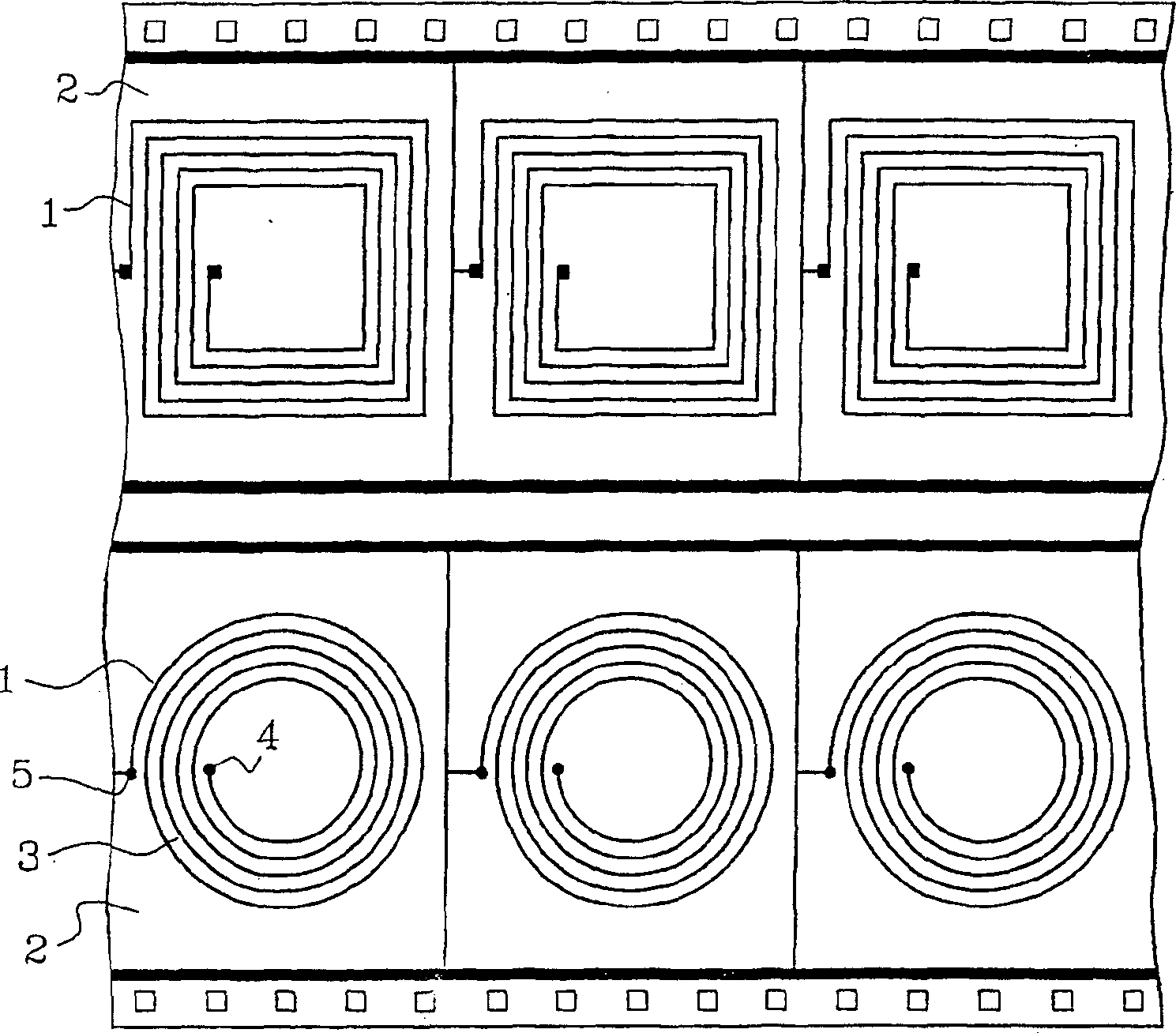
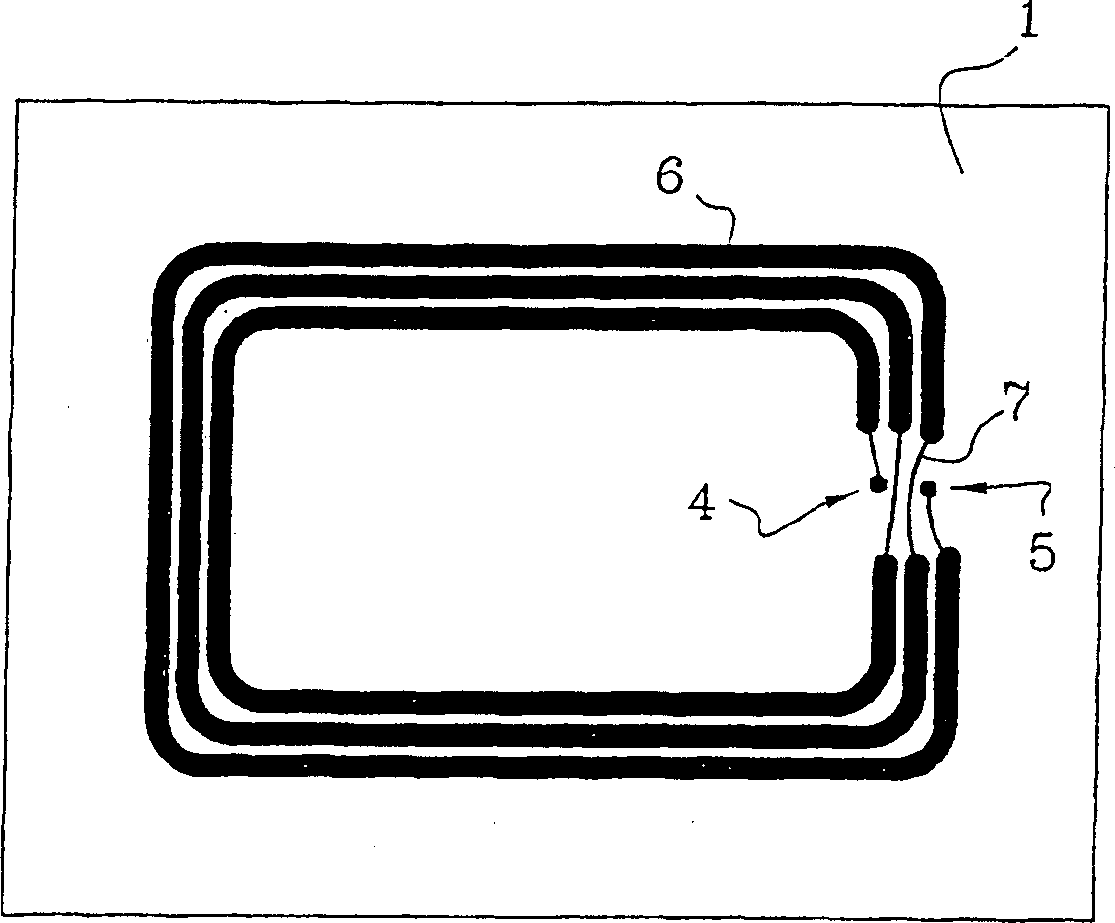
[0021] The manufacturing method according to the invention basically has two steps: in the first step, the pattern 1 of the circuit to be printed, i.e. in figure 1 The planar antenna in the case shown is coated on an insulating substrate 2 with conductive ink.

[0022] It has been found that not all conceivable printing methods are equally suitable for applying conductive ink.

[0023] According to the invention, a circuit pattern is produced on a gravure printed cylinder using electrochemical methods, chemical methods or laser etching methods. The conductive ink must be prepared in such a way that it is suitable for gravure printing from the viewpoint of the viscosity and other physical / chemical properties of the conductive ink. The electrical resistance of the circuit pattern produced by the gravure printing method is lower than that of the circuit pattern produced by other printing methods, so that an acceptable resistance is obtained for the final product with a thin meta...


PUM

PropertyMeasurementUnit
thicknessaaaaaaaaaa
diameteraaaaaaaaaa
surface areaaaaaaaaaaa

Abstract

In a method for the manufacture of a printed circuit on a dielectric carrier (2), in a first step a circuit pattern (1) is applied with an electrically conductive ink and, in a second step, the circuit model is plated, the electrically conductive ink being applied by means of a method of gravure printing and the plating being done by electrolytic or chemical means.

Description

technical field [0001] The invention relates to a method for producing a printed circuit on an insulating carrier, wherein a circuit pattern has a conductive ink applied on said insulating carrier, and the circuit obtained is then electroplated. The invention also relates to planar antennas manufactured by said method and their use in small swimming objects such as smart cards, electronic tags, circuits for wireless communication or the like. Background technique [0002] A method for producing printed circuits of the above-mentioned type is known from WO 99 / 52336. [0003] Cards known as smart cards or chip cards are widely used in the field of credit cards, ID cards or similar cards. These cards are cards in which user-related data can be stored. This smart card has flat contacts on one side. These flat contacts make mechanical contact with corresponding contacts in the smart card reader for reading and writing information. The query of data or the writing of data take...

Claims


Application Information

Patent Timeline
Patent Type & Authority Applications(China)
IPC IPC(8): G06K19/07G06K19/077H05K1/09H05K1/16H05K3/06H05K3/12H05K3/24H05K3/42
CPCH05K2203/1572H05K2203/0534H05K1/165H05K2203/0143H05K2203/1545H05K3/245G06K19/07779H05K2203/0113H05K3/1275H05K1/095G06K19/07783H05K2201/0347H05K3/246H01Q1/38
Inventor 克里斯托弗·玛瑟尤
Owner MICROCONNECTIONS
Why Eureka
Try Eureka