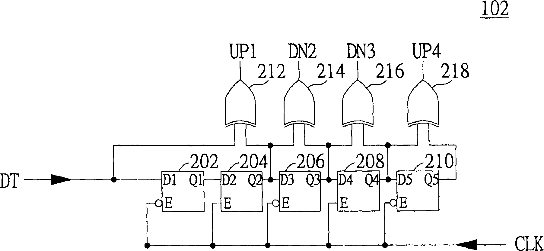
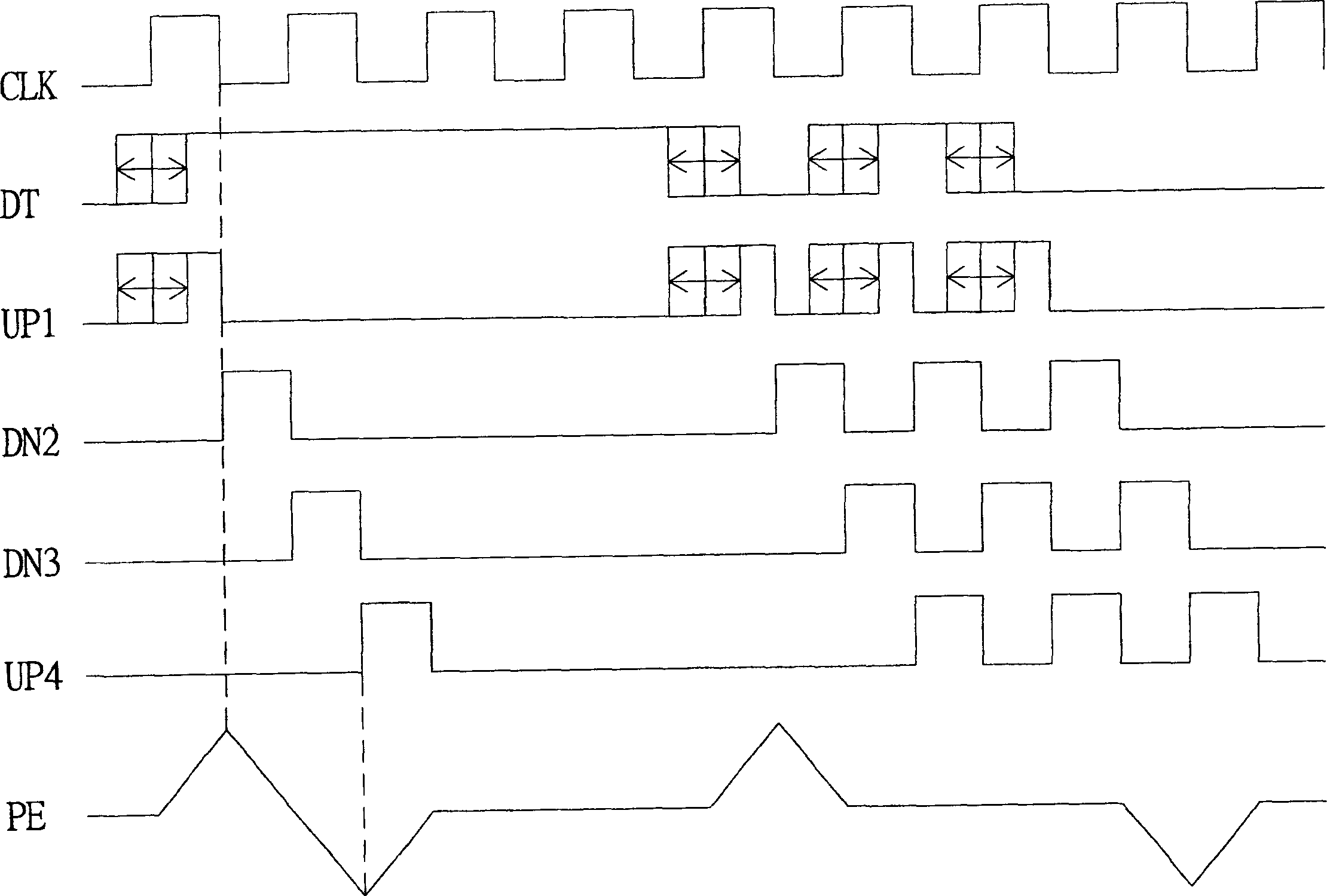
Phase detector
A phase detector and latch technology, applied in the direction of electrical components, automatic power control, etc., can solve the problem that the phase-locked loop clock recovery system cannot be locked
- Summary
- Abstract
- Description
- Claims
- Application Information
AI Technical Summary
Problems solved by technology
Method used
Image
Examples
Embodiment 1
[0048] Please refer to Figure 7 , Figure 7 The circuit block diagram of the phase detector of the first embodiment of the present invention is shown. The phase detector 700 of the present invention includes a first latch 702, a second latch 704, a third latch 706, a fourth latch 708, a fifth latch 710, and a sixth latch 712 , A first logic gate, a first SR-type latch 720, a second SR-type latch 722, a third SR-type latch 724, and a fourth SR-type latch 726. Among them, the first, second and third latches 702, 704 and 706, the first logic gate 730 and the first SR type latch 720 are combined to form a first rising signal generating circuit, which receives the data signal DT' and the clock The signal CLK' generates the first rising signal UP1'. The first to fourth latches 702 to 708 and the second SR-type latch 722 are combined to form a first falling signal generating circuit, which also receives the data signal DT' and the clock signal CLK' to generate the first falling signal D...
Embodiment 2
[0061] Please refer to Picture 10 , Picture 10 The circuit block diagram of the phase detector of the second embodiment of the present invention is shown. Different from the phase detector 700 of the first embodiment, the first rising signal generation circuit of the phase detector 1000 of the second embodiment also has a compensation circuit, which includes a seventh latch 1002, an eighth latch The register 1004, an OR logic gate 1008 and a second logic gate. The second logic gate is an AND logic gate 1006.
[0062] The seventh latch 1002 has a seventh input terminal D7 for receiving the data signal DT' and is enabled by the high level of the clock signal CLK'. The eighth latch 1004 has an eighth input terminal D8 for receiving the output signal of the seventh latch 1002 and is enabled by the low level of the clock signal CLK'. The AND logic gate 1006 is used to perform an AND logic operation on the inverted signal of the output signal of the eighth latch 1004 and the output si...
PUM
 Abstract
Description
Claims
Application Information


