Optical disc and optical disc address reading apparatus and method

一种光盘、地址的技术,应用在读取装置领域,能够解决串扰等问题

Inactive Publication Date: 2005-01-05
PANASONIC CORP
View PDF1 Cites 0 Cited by
  • Summary
  • Abstract
  • Description
  • Claims
  • Application Information

AI Technical Summary

Problems solved by technology

Moreover, if the track spacing is set narrow, crosstalk problems are prone to occur

Method used


Image

  • Optical disc and optical disc address reading apparatus and method
  • Optical disc and optical disc address reading apparatus and method
  • Optical disc and optical disc address reading apparatus and method

Examples


Embodiment 1

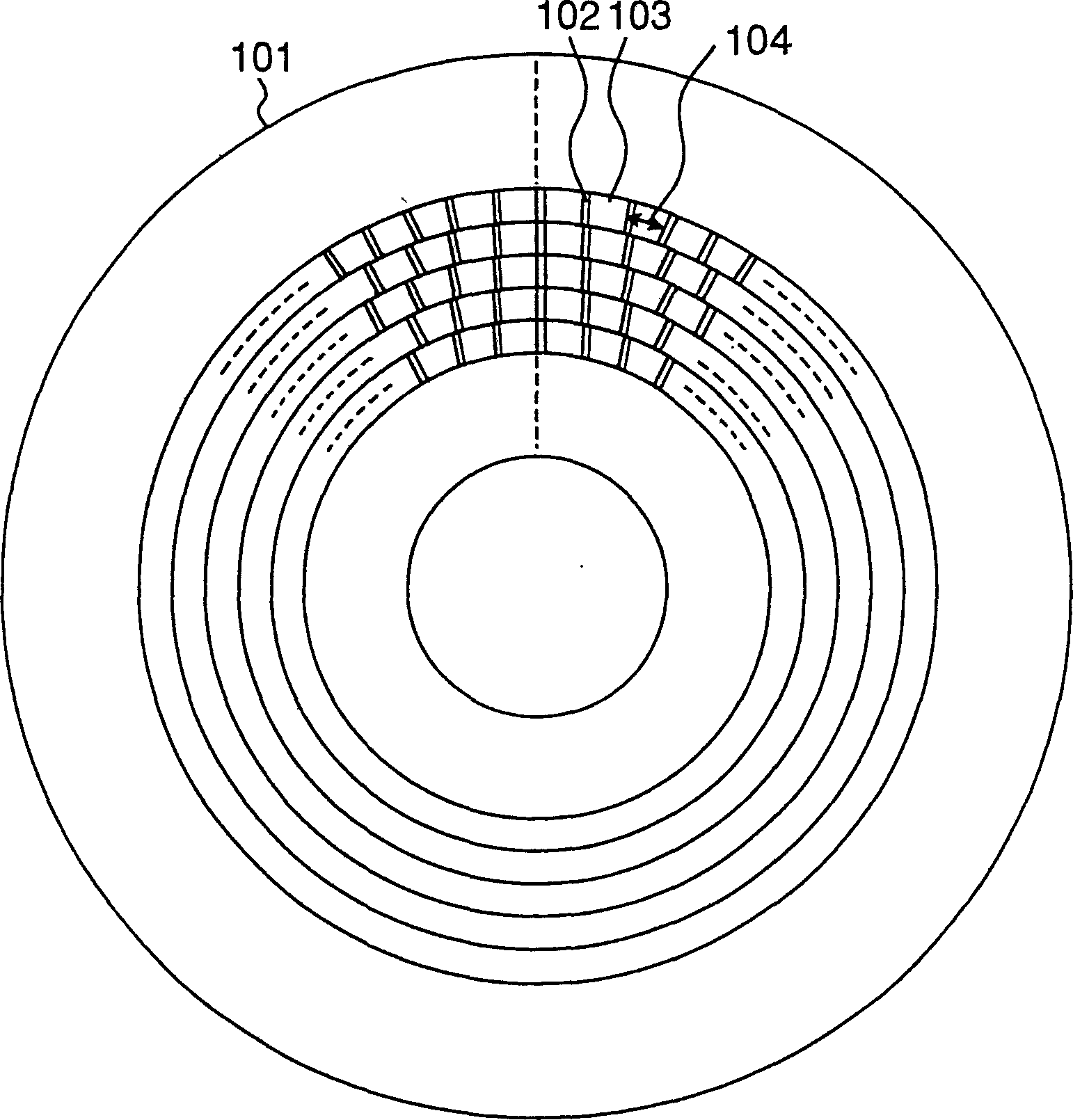
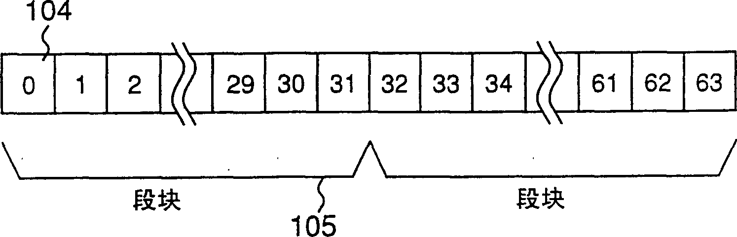
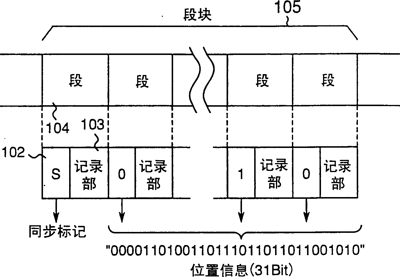
[0170] Figure 1A 1B is a structural diagram of an optical disc according to Embodiment 1 of the present invention, and 1B is an explanatory diagram showing the arrangement of segments. exist Figure 1A Among them, 101 is an optical disc substrate, 102 is a header portion formed in advance when manufacturing an optical disc, 103 is a recording portion where information can be recorded, and 104 is a segment which is an information unit of data. exist Figure 1B Among them, 105 means a segment block with a given number, for example, 32 as a unit.

[0171] On the optical disk substrate 101, a phase change film is formed in advance which optically changes the phase state like amorphous or crystalline, and reads a signal based on the difference in reflectance during recording and reproduction.

[0172] Below, refer to Figure 2A , detailing the relationship between segment 104 and segment block 105 .

[0173] In the optical disk of this embodiment, a track is formed by continuou...

Embodiment 2

[0218] In Example 2, instead of image 3 Groove discontinuities of varying widths shown, such as Figure 10 As shown, the discrete address is provided by utilizing the groove deformations, namely the groove lower offset 65 , the groove upper offset 66 , and their combination 67 . Such as Figure 10 As shown, the positive mark "1" is represented by the upper groove offset 66 alone, and the synchronization is represented by the combination 67 of the lower groove offset 65 and the upper groove offset 66 occurring in the following given time. The notation "S", if the groove lower excursion 65, and the groove upper excursion 66 does not occur within the following given time, represents a negative notation "0". The groove lower offset and the groove upper offset are collectively referred to as the groove offset. Any one of the part 65, the part 66, and the combination part 67 may be used as the synchronization mark, the positive mark, or the negative mark, but it is preferable to...

Deformed example 1

[0240] From Figure 15 to Figure 20 A first modification example of the groove deformation portion of the second embodiment is shown.

[0241] exist Figure 10 In, although the groove lower offset part 65 and the groove upper offset part 66 are used, but in Figure 17 In the first modified example, the groove descending phase inversion part 74 and the groove rising phase inverting part 75 are respectively changed. The groove falling inverting portion 74 is the descending portion of the groove that oscillates in a sinusoidal wave from the peak to the valley Even if the phase of about 1 / 4 of the swing cycle from the peak of the groove is reversed up and down, the groove rising inverting portion 75 is the rising portion from the valley to the peak of the groove even if the phase is reversed up and down for about 1 / 4 of the wobble period from the valley of the groove. The groove falling phase inverter and the groove rising phase inverter are collectively referred to as the groo...


PUM


Abstract

An optical disc having marks for dispersed addresses that can be easily detected with high precision. A dispersed address comprises synchronization marks, positive marks, and negative marks. Synchronization marks, positive marks, and negative marks are formed along a groove as partial discontinuities or partial modifications in the wobbled groove.

Description

technical field [0001] The present invention relates to an optically rewritable optical disc and a device and method for reading addresses written in advance on the optical disc. Background technique [0002] In recent years, there have been DVD-RAM, CD-RW, MD, etc. as optical discs on which users can record. These recordable optical discs are manufactured by forming grooves along spiral or concentric tracks and forming the surfaces of the grooves with phase change material or optomagnetic material. Furthermore, in order to specify the position on the optical disc, an address is recorded by reserving an unrewritable mark on the track. An example of such addresses is disclosed in JP-A-8-315426. [0003] According to JP-A-8-315426, a discontinuous portion is provided in a groove, and the discontinuous portion is formed in a pattern corresponding to an address signal. Here, the pattern corresponding to the address signal refers to a binarized signal that is inverted every ti...

Claims


Application Information

Patent Timeline
Patent Type & Authority Applications(China)
IPC IPC(8): G11B7/007G11B7/00G11B7/0037G11B7/24073G11B7/24082G11B20/10G11B20/12G11B20/14G11B20/18G11B27/10G11B27/19G11B27/24G11B27/30
CPCG11B20/1833G11B27/105G11B7/007G11B2020/1292G11B2220/20G11B20/1403G11B2220/2545G11B20/00601G11B2220/2529G11B27/3027G11B27/19G11B7/00G11B2220/2575G11B20/12G11B20/1217G11B2020/1298G11B7/00745G11B20/10009G11B2220/216G11B2020/1287G11B2020/1268G11B2020/1239G11B2020/1232G11B7/0037G11B2020/1269G11B27/24G11B20/1252G11B7/0943G11B20/10231G11B7/127G11B20/10268G11B2220/2537G11B2007/00754G11B2020/1267
Inventor 古宫成石桥广通石田隆小林良治
Owner PANASONIC CORP
Why Eureka
Try Eureka