Long wavelength vertical cavity surface emitting laser with integrated photodetector

A surface emission, photodetector technology, applied in lasers, semiconductor lasers, laser parts and other directions, can solve the problem of high percentage

Inactive Publication Date: 2005-02-23
SAMSUNG ELECTRONICS CO LTD
View PDF1 Cites 12 Cited by
  • Summary
  • Abstract
  • Description
  • Claims
  • Application Information

AI Technical Summary

Problems solved by technology

However, the percentage of spontaneous emission received by the entire area of ​​the photodetector is high

Method used


Image

  • Long wavelength vertical cavity surface emitting laser with integrated photodetector
  • Long wavelength vertical cavity surface emitting laser with integrated photodetector
  • Long wavelength vertical cavity surface emitting laser with integrated photodetector

Examples


Embodiment Construction

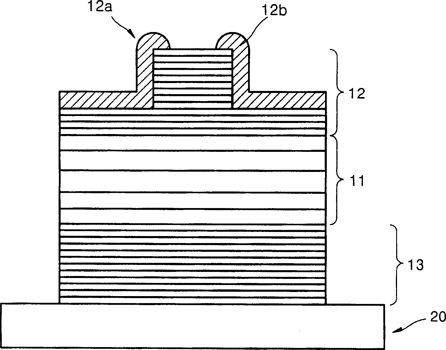
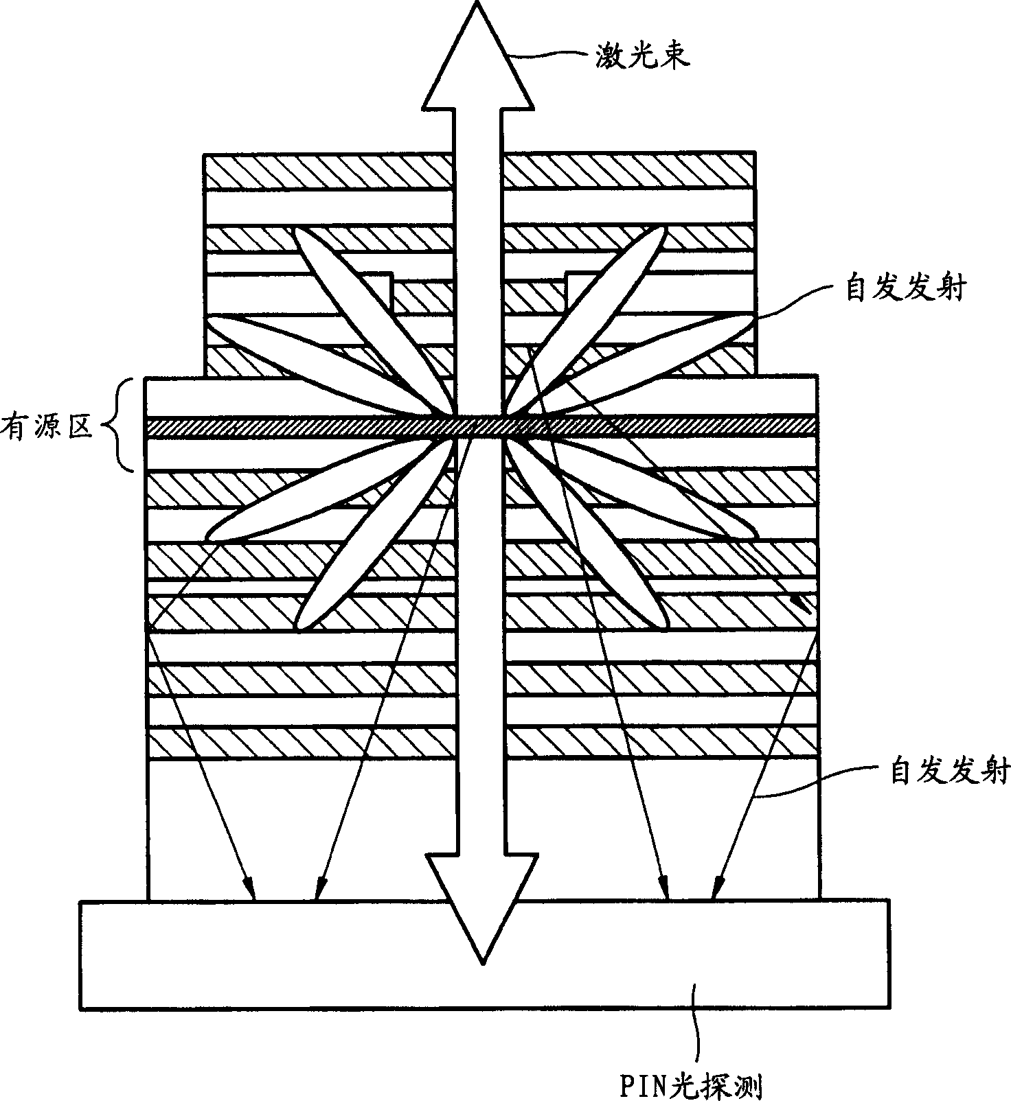
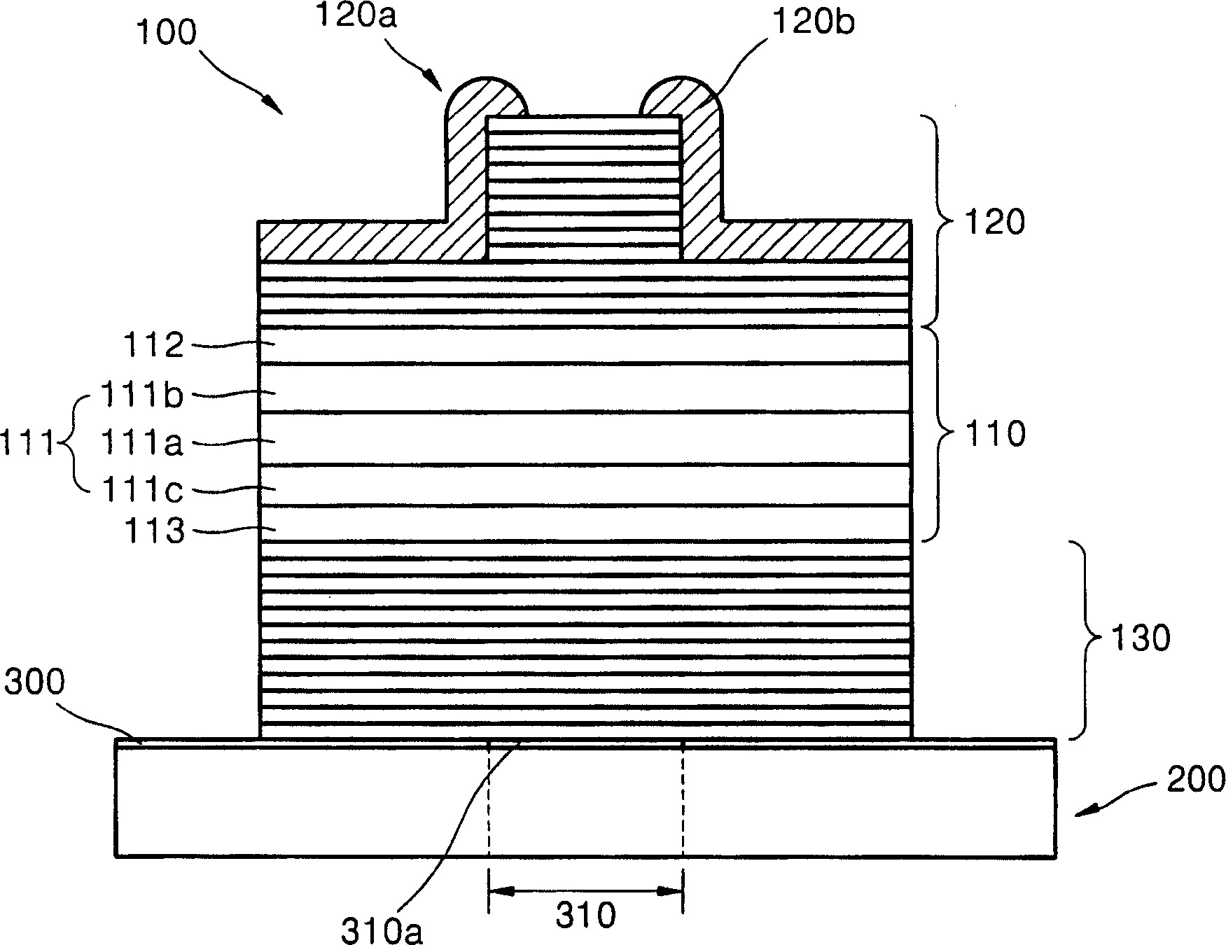
[0018] image 3 A vertical cavity surface emitting laser (VCSEL) is schematically shown in which a ridge is formed on an upper semiconductor layer. The VCSEL is a well-known laser emitting structure, which includes an active region where laser emission occurs, and upper and lower semiconductor layers with the active region interposed therebetween. Thus, the following detailed description of the laser emitting structure does not limit the technical scope of the present invention.

[0019] Such as image 3 As shown, the laser emitting structure 100 includes: an active region 110, which is a cavity for generating laser resonance; and upper and lower semiconductor layers 120 and 130 of a distributed Bragg reflector (DBR), with the active region interposed therebetween 110. The lower semiconductor layer 130 includes a substrate (not shown). The active region 110 includes an active layer 111 and capping layers 112 and 113 with the active layer 111 interposed therebetween. The a...


PUM

PropertyMeasurementUnit
widthaaaaaaaaaa

Abstract

A vertical cavity surface emitting laser (VCSEL) integrated with a photodetector is provided. The photodetector is attached to a bottom surface of the VCSEL by a bonding layer, which includes a window of a predetermined diameter. The bonding layer is a eutectic bonding layer. An air gap exists within the window and mainly transmits a laser beam. Most of spontaneous emission light incident at an angle is blocked by an area of the bonding layer other than the window, and even some of the spontaneous emission light that heads toward the window cannot easily passes through the window due to a big difference between refractive indices of a semiconductor layer and the air. Thus, the eutectic bonding layer greatly reduces a voltage drop at an interface between the VCSEL and the photodetector, thereby contributing to mass production.

Description

technical field [0001] The present invention relates to a long wavelength Vertical Cavity Surface Emitting Laser (VCSEL) with an integrated photodetector. Background technique [0002] Typically, VCSEL diodes are combined with photodetectors for power monitoring and automatic power control (APC) based on power monitoring. For example, in US Patent No. 5,943,357, photodetectors are attached to long wavelength VCSELs by wafer fusion. [0003] figure 1 A simplified cross-sectional view of a conventional VCSEL fused with a photodetector. refer to figure 1 A conventional VCSEL includes an upper semiconductor layer 12 of a Distributed Bragg Reflector (DBR), an active region 11 and a lower semiconductor layer 13 of the DBR sequentially deposited on a substrate (not shown). The active region 11 is the cavity where the central laser resonance occurs. The PIN photodetector 20 is fused or bonded to the bottom of the VCSEL with this structure. [0004] As mentioned above, a photod...

Claims


Application Information

Patent Timeline
Patent Type & Authority Applications(China)
IPC IPC(8): G11B7/125H01L31/147H01S5/02H01S5/026H01S5/0683H01S5/183
CPCB82Y10/00H01S5/18375H01S5/0683H01S5/18377H01S5/0264H01S5/18308H01L31/147B82Y20/00H01S5/183
Inventor 金泽
Owner SAMSUNG ELECTRONICS CO LTD
Why Eureka
Try Eureka