Lead on chip semiconductor package and producing method and equipment thereof

A semiconductor and chip technology, applied in semiconductor/solid-state device manufacturing, semiconductor devices, semiconductor/solid-state device components, etc., can solve problems such as deterioration of lead 12 flatness, contamination of I/O pads, etc.

Inactive Publication Date: 2005-09-28
SAMSUNG ELECTRONICS CO LTD
View PDF0 Cites 1 Cited by
  • Summary
  • Abstract
  • Description
  • Claims
  • Application Information

AI Technical Summary

Problems solved by technology

[0015] However, there is still a gap between the chip 11 and the lead 12, and the liquid adhesive 31 will further deteriorate the flatness of the lead 12
Additionally, the flowable liquid adhesive 31 may contaminate the I / O pads ( figure 1 and 2 11a) in

Method used


Image

  • Lead on chip semiconductor package and producing method and equipment thereof
  • Lead on chip semiconductor package and producing method and equipment thereof
  • Lead on chip semiconductor package and producing method and equipment thereof

Examples


Embodiment Construction

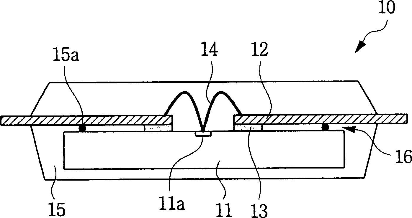
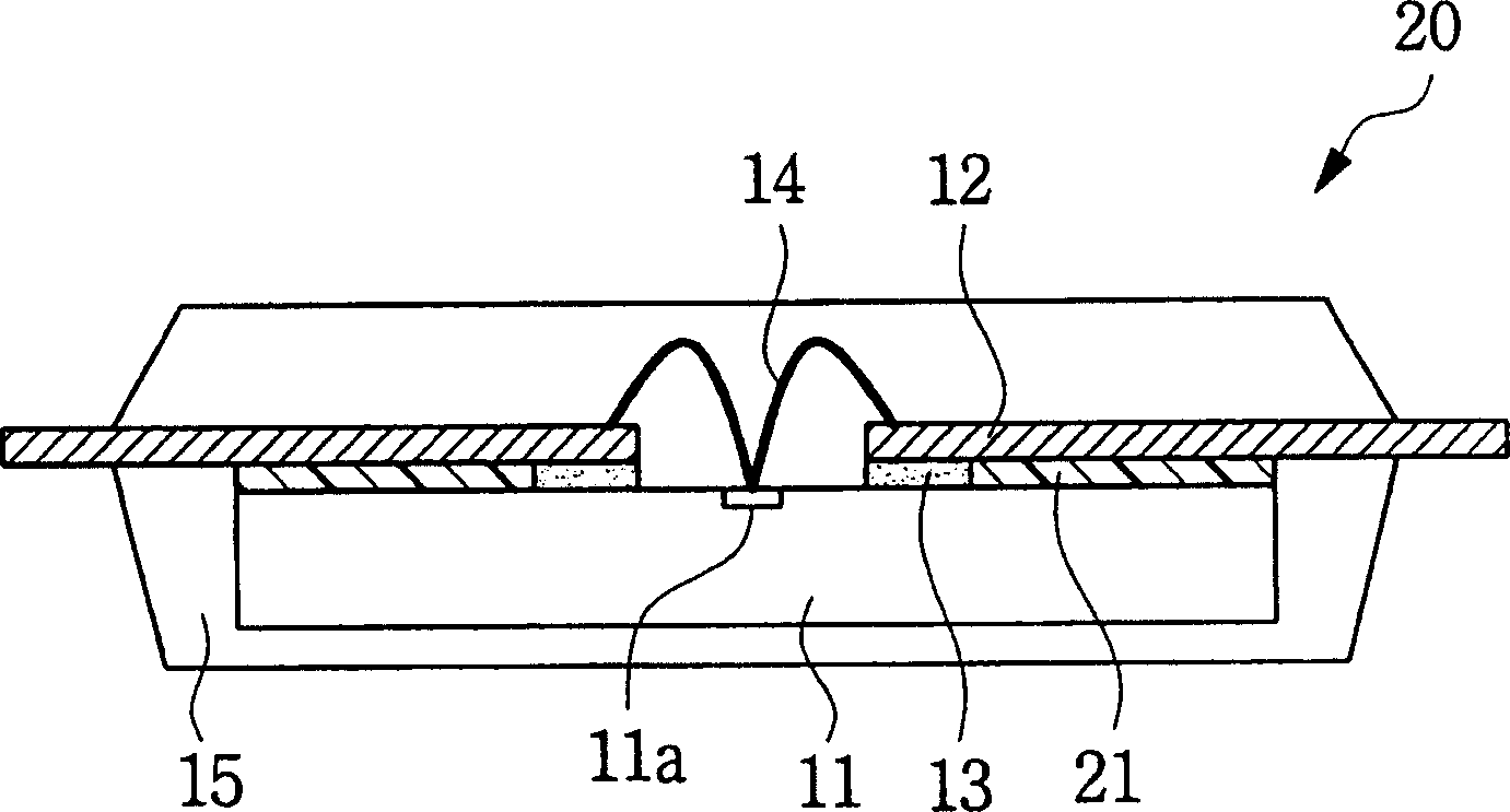
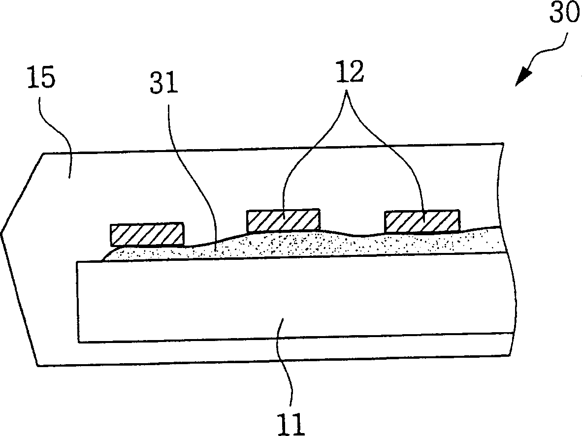
[0061] Exemplary and non-limiting embodiments of the present invention will be described more fully hereinafter with reference to the accompanying drawings. This invention may, however, be embodied in many different forms and should not be construed as limited to the exemplary embodiments set forth herein. Rather, the disclosed embodiments will enable those skilled in the art to complete and complete this disclosure and fully convey the scope of the invention. The principles and features of this invention may be employed in varied and numerous embodiments without departing from the scope of the invention.

[0062] Note that well-known structures and processes are not described or illustrated in detail to avoid obscuring the gist of the present invention. Note also that the drawings are not drawn to scale. Conversely, the dimensions of some of the elements are exaggerated relative to other elements for simplicity and clarity of illustration. Like reference numerals are used ...


PUM


Abstract

Used for semiconductor packing, an adhesive agent (130) is used on parts of a conductor framework (120) and on parts of a specific surface on an integrated switching circuit chip (ISCC) so as to hold the conductor framework on the ISCC. A majority of input/output contact points (112) are located on the top side of the ISCC. Independent claims are also included for the following: (A) A method for producing semiconductor packing; (B) and for a device for producing semiconductor packing.

Description

technical field [0001] The present invention mainly relates to semiconductor packaging technology, and more particularly, to a semiconductor package in which leads of a lead frame are in direct contact with and attached to the surface of an integrated circuit chip, and related manufacturing methods and devices. Background technique [0002] Semiconductor packaging refers to the casing and interconnection of integrated circuits (ICs), also known as chips or dies, which form an electronic system after packaging. The functions provided by the package may include a structure to mechanically support the chip, a physical enclosure to protect the chip from the environment, electrical connections to allow signals and power to flow in and out of the chip, and appropriate means to remove heat generated by the chip or system. Leadframes are often used in packages to provide mechanical support, electrical connections, and thermal paths for the chip. [0003] Various leadframe packages ...

Claims


Application Information

Patent Timeline
Patent Type & Authority Applications(China)
IPC IPC(8): H01L23/50H01L21/50H01L21/56H01L21/58H01L21/60H01L23/16H01L23/32H01L23/495
CPCH01L2224/45124H01L24/45H01L2224/4826H01L2924/01004H01L24/48H01L2924/01079H01L2924/01068H01L2224/32245H01L24/32H01L2224/48247H01L2224/73215H01L2924/14H01L2924/01005H01L2924/01033H01L23/4951H01L2924/01078H01L2924/01014H01L23/49558H01L2224/45144H01L2224/48091H01L2224/73265H01L2924/01013H01L2924/351H01L2924/181H01L24/73H01L2924/00014H01L2924/00012H01L2924/3512H01L2924/00
Inventor 李灿石吴世容金震镐李相协郭旻根尹盛焕南太德
Owner SAMSUNG ELECTRONICS CO LTD
Why Eureka
Try Eureka