Method of making a lead-on-chip device

a technology of lead-on-chip and plastic molding, which is applied in the direction of semiconductor devices, semiconductor/solid-state device details, electrical equipment, etc., can solve the problems of total exfoliation, cracks in semiconductor chips, and increasing in size of applications

Inactive Publication Date: 2005-07-05
LAPIS SEMICON CO LTD
View PDF17 Cites 1 Cited by
  • Summary
  • Abstract
  • Description
  • Claims
  • Application Information

AI Technical Summary

Benefits of technology

[0015]According to an aspect of the present invention, there is provided a semiconductor device comprising: a semiconductor chip including a top side and a bottom side; a package including an upper portion provided on the top side of the semiconductor chip and a lower portion provided on the bottom side thereof, the upper portion being thicker than the lower portion; and a resisting member provided on the bottom side of the semiconductor chip, for preventing the semiconductor chip from being bent.
[0019]According to still another aspect of the present invention, there is provided a semiconductor device having a plurality of leads formed on a semiconductor chip comprising: a semiconductor chip including a top side and a bottom side; a package including an upper portion provided on the top side of the semiconductor chip and a lower portion provided on the bottom side thereof, the upper portion being thicker than the lower portion; and a resisting member provided on the bottom side of the semiconductor chip, for preventing the semiconductor chip from being bent.
[0020]According to still another aspect of the present invention, there is provided a semiconductor device, the thickness of which is below a given value regulated by a specification of Thin Small Outline Package, comprising: a semiconductor chip including a top side and a bottom side; a package including an upper portion provided on the top side of the semiconductor chip and a lower portion provided on the bottom side thereof, the upper portion being thicker than the lower portion; and a resisting member provided on the bottom side of the semiconductor chip, for preventing the semiconductor chip from being bent.
[0021]According to still another aspect of the present invention, there is provided a method of manufacturing a semiconductor device including a semiconductor chip and a package sealing the semiconductor chip, the semiconductor chip having a top side and a bottom side, and a plurality of leads being arranged on the top side of the semiconductor chip, the method comprising: forming a resisting member on the bottom side of the semiconductor chip, for preventing the semiconductor chip from being bent.
[0022]According to still another aspect of the present invention, there is provided a semiconductor device, having a thickness below a given value regulated by a specification of Thin Small Outline Packages, comprising: a semiconductor chip including a top side and a bottom side; a package including an upper portion provided on said top side of the semiconductor chip and a lower portion provided on said bottom side thereof, said upper portion being thicker than said lower portion; and a resisting member provided on said bottom side of said semiconductor chip, for preventing said semiconductor chip from being bent.

Problems solved by technology

On the other hand, appliances tend to be increasingly smaller in size, which requires the semiconductor devices to be smaller.
However, a total exfoliation might yield a crack in the semiconductor chip 91 or in the plastic sealing layer 97.
If water is absorbed in the semiconductor device, the water will vaporize to yield a crack therein.
As discussed above, the conventional LOC semiconductor device has such drawbacks that they may cause a crack in the semiconductor ship or in the plastic sealing layer.

Method used


Image

  • Method of making a lead-on-chip device
  • Method of making a lead-on-chip device
  • Method of making a lead-on-chip device

Examples


first embodiment

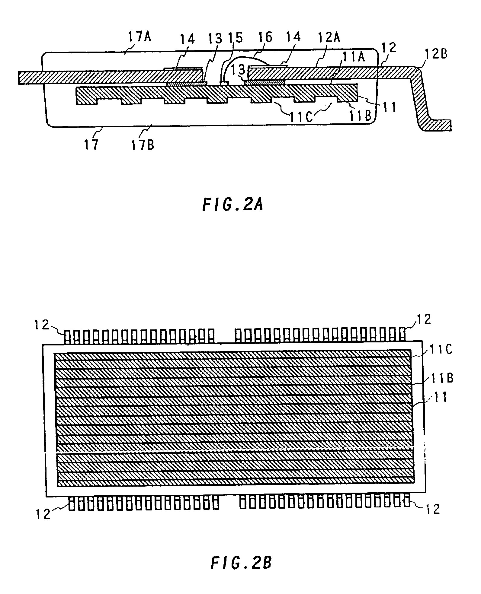
[0041]FIG. 2A is a cross sectional view of the semiconductor device of the first embodiment and FIG. 2B shows the bottom of the semiconductor chip mounted in the semiconductor device.

[0042]The semiconductor device is an LOC (Lead On Chip) semiconductor device, and in particular, a TSOP (Thin Small Outline Package) semiconductor device. Therefore, the thickness of the semiconductor device is required to be below 1.27 mm as explained above.

[0043]The semiconductor device incorporates a semiconductor chip 11, a plurality of leads 12, a plurality of insulation tapes 13, a plurality of electrode pads 15, a plurality of bonding wires 16, and a plastic sealing layer 17. Examples of the materials used for these components are as follows. The insulation tapes 13 are made of a thermoplastic resin, wherein both the top side and the bottom side of the insulation tapes 13 are adhesive. The electrode pads 15 are made of Ni—Fe and Cu. The bonding wires 16 are made of alloy.

[0044]On the top side 11A...

second embodiment

[0049]the semiconductor device according to the present invention will now be described.

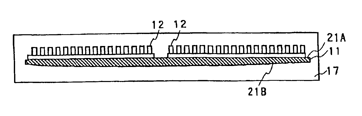
[0050]FIG. 3A is a cross sectional view of the semiconductor device of the second embodiment, and FIG. 3B shows the bottom of the semiconductor chip mounted in the semiconductor device of the second embodiment. The principal feature of the second embodiment is that the thickness of the center portion of the semiconductor chip is greater than that of the other portions. In other words, the main feature is that the semiconductor chip has a curved bottom.

[0051]The components of the semiconductor device according to the second embodiment are almost the same as those of the semiconductor device according to the first embodiment; therefore, for ease of explanation, a discussion of the feature of the second embodiment will be made below. In FIG. 3A, the semiconductor chip 11 has a curved or convex shape. The convex portion of the semiconductor chip 11 acts as a resisting member for preventing the semico...

third embodiment

[0053]the semiconductor device according to the present invention will now be described in detail.

[0054]FIG. 4A is a cross sectional view of the semiconductor device of the third embodiment, and FIG. 4B shows the bottom of the semiconductor chip mounted in the semiconductor device. The components of the semiconductor device of the third embodiment are almost the same as those of the semiconductor device of the first embodiment. Therefore, the distinguishing feature of the third embodiment will principally be discussed below.

[0055]The third embodiment is distinguished in that an adhesive 22 is applied between the semiconductor chip 11 and the plastic sealing layer 17, such that the adhesive 22 serves to prevent the semiconductor chip 11 from being warped or bent. Specifically, the adhesive 22 is made of polyimide resin. In FIGS. 4A and 4B, the entire bottom side of the semiconductor chip 11 is coated with the polyimide resin 22 to avoid exfoliation of the semiconductor chip 11 from t...


PUM


Abstract

A semiconductor device which is sealed with a plastic sealing layer and whose thickness is regulated to be below a given value is known. Since the thickness of the device is small, and the thickness of the upper portion of the plastic sealing layer and the thickness of the lower portion thereof are different from each other, the plastic sealing layer becomes warped, thus causing a crack on the side of the semiconductor chip.To solve this problem, the semiconductor device according to the present invention comprises a semiconductor chip on which a plurality of grooves are defined. Consequently, the thickness of the lower portion of the plastic layer becomes greater, thereby preventing cracks from occurring on the semiconductor chip.

Description

[0001]This application is a divisional of U.S. application Ser. No. 09 / 328,905, filed Jun. 9, 1999 now U.S. Pat. No. 6,534,845.[0002]This patent application claims priority based on a Japanese patent application, H10-295817 filed on Oct. 16, 1998, the contents of which are incorporated herein by reference.BACKGROUND OF THE INVENTION[0003]1. Field of the Invention[0004]The present invention relates to a plastic molding seal semiconductor device, and in particular to an LOC (Lead on Chip) type semiconductor.[0005]2. Description of the Related Art[0006]Plastic molding seal semiconductor devices for electronic equipment have been widely used. These semiconductor devices are sealed with plastic to protect the semiconductor chips laid in the semiconductor devices. Recently, these semiconductor devices, especially LSIs (Large Scaled Integrated circuits) have increased in size with the enhancement of integration. For example, the storage capacity of memory devices is increasing, so that the...

Claims


Application Information

Patent Timeline
Patent Type & Authority Patents(United States)
IPC IPC(8): H01L23/495H01L29/06H01L29/02H01L23/48H01L21/56H01L23/29H01L23/31H01L23/50
CPCH01L23/4951H01L24/06H01L29/0657H01L2224/04042H01L2224/05647H01L2224/05655H01L2224/06136H01L2224/48091H01L2224/48247H01L2224/4826H01L2224/48465H01L2224/49171H01L2224/73215H01L2924/01004H01L2924/01029H01L2924/01078H01L2924/01082H01L2924/10158H01L2924/14H01L2924/00014H01L2924/01026H01L2924/01005H01L2924/01033H01L2924/00H01L24/48H01L24/49H01L2224/32245H01L2924/00012H01L2224/05554H01L2224/05599H01L2224/85399H01L2224/854H01L2924/10155H01L2924/181H01L2924/351H01L2224/45015H01L2924/207H01L2224/45099
Inventor YAMADA, ETSUONAGASAKI, KENJISHIRAISHI, YASUSHISERA, KAZUHIKO
Owner LAPIS SEMICON CO LTD
Why Eureka
Try Eureka