Semiconductor device

a semiconductor device and semiconductor technology, applied in the direction of printed circuit assembling, printed circuit non-printed electric component association, printed circuit manufacturing, etc., can solve the problems of package cracking, weak semiconductor device, reliability drop, etc., and achieve the effect of efficiently cooling the individual semiconductor device and reducing the above-mentioned parasitic capacity

Inactive Publication Date: 2005-07-19
RENESAS TECH CORP
View PDF52 Cites 0 Cited by
  • Summary
  • Abstract
  • Description
  • Claims
  • Application Information

AI Technical Summary

Benefits of technology

[0133]According to the means of the foregoing item 44, the semiconductor devices of the means of each of the foregoing items 40 to 43 are so packed in their mounting substrates that their radiating grooves merge into each other. The cooling draft can be established in the direction of the radiating grooves and the second rad...

Problems solved by technology

Because of the large stray capacity between the inner leads and the semiconductor chip, the semiconductor device has a problem that the signal transmission rate is drooped by the large stray capacity to increase the electrical noises.(2) Because of the large area of the insulating films, the amount of moisture absorbed is increased so that the absorbed moisture is gasified and expanded in the package during the reflow, thus causing a problem that the package cracking is established by the moisture expansion.(3) Since the aforementioned insulating films are made of a resin of polyimide, the amount of absorbed moisture is increased so that the absorbed moisture is gasified and expanded in the package during the reflow, thus causing the problem of package cracking.(4) Since the aforementioned adhesive as made of an acrylic resin, it is degraded by the pressure cracker test or the like, thus raising a problem that the reliability is dropped by the electrical leakage between the leads and the corrosions of the aluminum electrodes.(5) Since the circuit forming surface of the semiconductor chip is not coated all over with the resin coating of polyimide for protect...

Method used


Image

  • Semiconductor device
  • Semiconductor device
  • Semiconductor device

Examples


embodiment i

(Embodiment I)

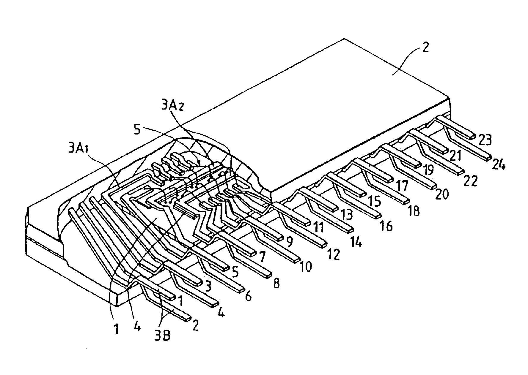
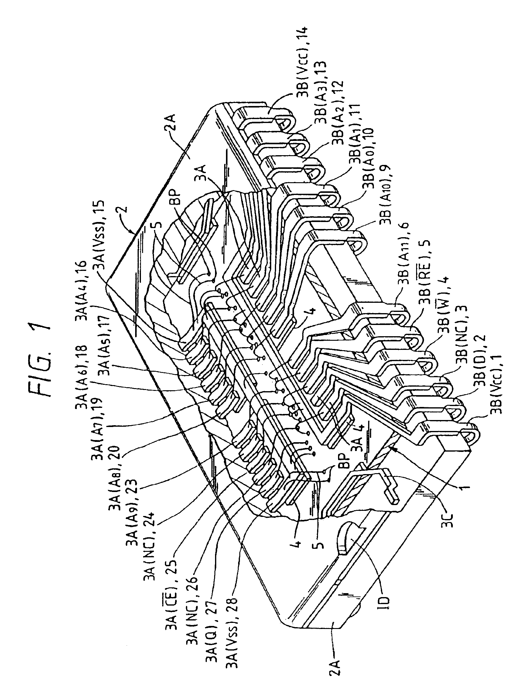
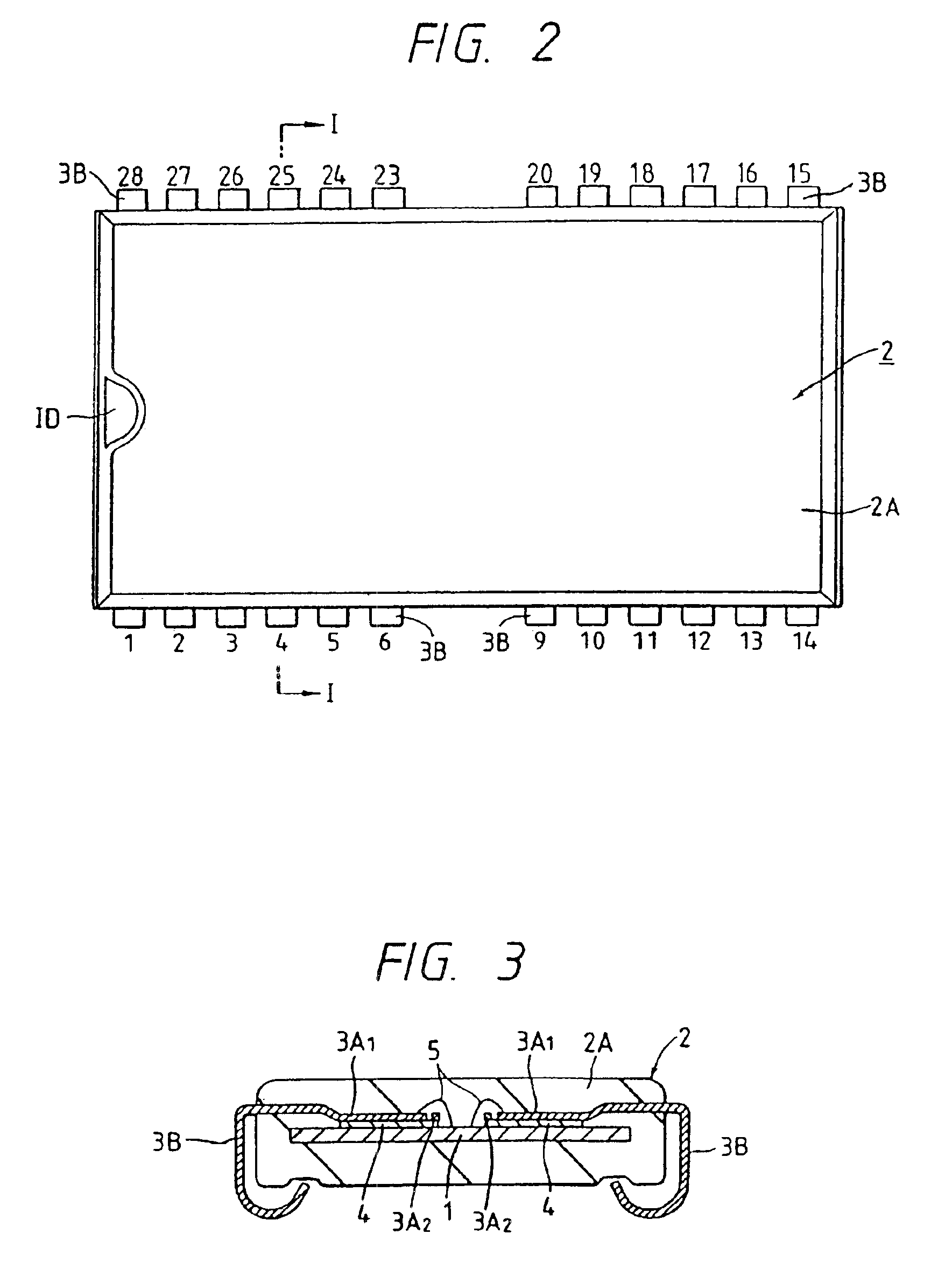
[0190]A resin-sealed type semiconductor device or sealing a DRAM according to the embodiment I of the present invention is shown in FIG. 1 (in partially sectional perspective view), in FIG. 2 (in top plan view) and in FIG. 3 (in section taken along line I—I of FIG. 2).

[0191]As shown in FIGS. 1, 2 and 3, a DRAM (i.e., a semiconductor chip) 1 is sealed with an SOJ (Small Out-line J-bend) type resin-sealed package 2. The DRAM 1 is made to have a large capacity of 16 (Mbits)×1 (bit) and a rectangular area of 16.48 (mm)×8.54 (mm). This DRAM 1 is sealed with the resin-sealed package 2 of 400 (mil).

[0192]The DRAM 1 has its principal surface arranged mainly with a memory cell array and a peripheral circuit. The memory cell array is arranged in a matrix form with a plurality of memory cells (or elements) for storing information of 1 (bit), as will be described in detail hereinafter. The peripheral circuit is comprised of a direct peripheral circuit and an indirect peripheral ci...

embodiment ii

(Embodiment II)

[0291]In the semiconductor integrated circuit device according to the Embodiment II of the present invention is constructed, as shown in FIG. 20, FIGS. 21A and 21B and FIGS. 22A and 22B, the insulating films 4 adhered to the principal surface of the semiconductor chip 1 of the foregoing Embodiment I are modified such that insulating films 4A are arranged all over or partially of those sides of the signal inner leads 3A1 and the common inner leads 3A2, which are located in the closest position to face the semiconductor chip 1.

[0292]More specifically, as shown in FIG. 20, the aforementioned insulating films 4A are placed in advance all over the most closest sides of the signal inner leads 3A1 and the common inner leads 3A2 facing the principal surface of the semiconductor chip 1 and are then fixedly adhered to the semiconductor chip 1, when assembled.

[0293]The lead frame 3 thus carrying the insulating films 4A is manufactured altogether with the signal inner leads 3A1 t...

embodiment iii

(Embodiment III)

[0306]In the semiconductor integrated circuit device according to the Embodiment III of the present invention, as shown in FIG. 23, the whole region of the principal surface of the semiconductor chip 1 except the bonding pads BP of the principal surface of the semiconductor chip 1 of the foregoing Embodiment I is coated with an alpha ray shielding polyimide film 8, and the principal surface of the semiconductor chip 1 further formed with insulating films 4D on its portions to which at least the signal inner leads 3A1 and the common inner leads 3A2 are to be adhered.

[0307]The alpha ray shielding polyimide film 8 has a thickness of 2.0 to 10.0 microns.

[0308]The insulating films 4D have a thickness of 75 microns or more. The resin suited or the insulating films 4D is exemplified by a thremoset resin containing a printable inorganic filler.

[0309]The area occupied by the insulating films 4D is at most one half of that of the semiconductor chip 1.

[0310]The semiconductor ch...


PUM


Abstract

As the semiconductor chip is large-sized, highly integrated and speeded up, it becomes difficult to pack the semiconductor chip together with leads in a package. In view of this difficulty, there has been adopted the package structure called the “Lead-On-Chip” or “Chip-On-Lead” structure in which the semiconductor and the leads are stacked and packed. In the package of this structure, according to the present invention, the gap between the leading end portions of the inner leads and the semiconductor chip is made wider than that between the inner lead portions except the leading end portions and the semiconductor chip thereby to reduce the stray capacity, to improve the signal transmission rate and to reduce the electrical noises.

Description

CROSS-REFERENCE TO RELATED APPLICATIONS[0001]This application is a divisional application of application Ser. No. 10 / 322,672, filed Dec. 19, 2002, now U.S. Pat. No. 6,720,208 which is a divisional application of Ser. No. 09 / 558,105, filed Apr. 25, 2000, now U.S. Pat. No. 6,531,760, issued Mar. 11, 2003, which is a divisional application of Ser. No. 09 / 288,673, filed Apr. 9, 1999, now U.S. Pat. No. 6,081,023, issued Jun. 27, 2000, which is a continuation application of Ser. No. 09 / 052,981, filed Apr. 1, 1998, now U.S. Pat. No. 5,914,530, issued Jun. 22, 1999, which is a divisional application of Ser. No. 08 / 646,031, filed May 7, 1996, now U.S. Pat. No. 5,793,099, issued Aug. 11, 1998, which is a continuation application of Ser. No. 08 / 293,555, filed Aug. 22, 1994, now U.S. Pat. No. 5,530,286, issued Jun. 25, 1996, which is a divisional application of Ser. No. 07 / 990,272, filed Dec. 14, 1992, now U.S. Pat. No. 5,358,904, issued Oct. 25, 1994, which is a divisional application of Ser. ...

Claims


Application Information

Patent Timeline
IPC IPC(8): H01L29/06H01L23/28H01L23/31H01L23/495H01L29/02H01L23/48H01L25/10H05K1/18H05K1/14H05K3/34H01L21/52H01L23/50
CPCH01L23/3107H01L23/4951H01L23/49555H01L23/49558H01L23/49568H01L23/49586H01L24/32H01L24/49H01L25/105H01L29/0657H01L2924/00014H01L2924/0132H01L2224/29111H01L2924/3511H01L2924/15738H01L2924/15747H01L2924/1576H01L2224/2929H01L2225/1088H01L2225/1029H01L2225/107H01L2224/2919H01L2225/1005H01L2224/48599H01L2224/48699H01L2224/48799H01L2924/10253H01L2224/0401H01L2924/07802H01L24/45H01L2224/05599H01L2224/32245H01L2224/45124H01L2224/45144H01L2224/45147H01L2224/4554H01L2224/4569H01L2224/48091H01L2224/48247H01L2224/4826H01L2224/48465H01L2224/49171H01L2224/73215H01L2224/85205H01L2224/85399H01L2224/8592H01L2224/92147H01L2924/01002H01L2924/01005H01L2924/01006H01L2924/01011H01L2924/01013H01L2924/01014H01L2924/01015H01L2924/01028H01L2924/01029H01L2924/0103H01L2924/01039H01L2924/01047H01L2924/0105H01L2924/01051H01L2924/01058H01L2924/01074H01L2924/01075H01L2924/01079H01L2924/01082H01L2924/01092H01L2924/13091H01L2924/14H01L2924/1815H01L2924/3025H05K1/144H05K1/181H05K3/3421H01L24/48H01L2224/16245H01L2224/73265H01L2924/01019H01L2924/01023H01L2924/01033H01L2924/01043H01L2924/01045H01L2924/014H01L2924/00012H01L2924/00H01L2924/01026H01L2924/3512H01L2924/0695H01L2924/181H01L2224/05554H01L2224/2612
Inventor MURAKAMI, GENTSUBOSAKI, KUNIHIROICHITANI, MASAHIRONISHI, KUNIHIKOANJO, ICHIRONISHIMURA, ASAOKITANO, MAKOTOYAGUCHI, AKIHIROKAWAI, SUEOOGATA, MASATSUGUEGUCHI, SYUUJIKOKAKU, HIROYOSHISEGAWA, MASANORIHOZOJI, HIROSHIYOKOYAMA, TAKASHIKINJO, NORIYUKIKANEDA, AIZOSAEKI, JUNICHINAKAMURA, SHOZOHASEBE, AKIOKIKUCHI, HIROSHIYOSHIDA, ISAMUYAMAZAKI, TAKASHIOSHIMA, KAZUYOSHIMATSUMOTO, TETSURO
Owner RENESAS TECH CORP
Why Eureka
Try Eureka