Preparation method of large diameter zone melting silicon single crystal

A zone melting single crystal furnace and zone melting silicon technology are applied in the field of large-diameter zone melting silicon single crystal preparation, and can solve problems such as being unable to be successfully realized.

Active Publication Date: 2006-01-25
ZHONGHUAN ADVANCED SEMICON MATERIALS CO LTD +1
View PDF0 Cites 14 Cited by
  • Summary
  • Abstract
  • Description
  • Claims
  • Application Information

AI Technical Summary

Problems solved by technology

As we all know, using the traditional preparation method of small-diameter zone-melting silicon single crystals below 3″, it is impossible to prepare large-diameter zone-melting silicon single crystals above 3″, especially 5″ and 6″ zone-melting silicon single crystals.

Method used


Image

  • Preparation method of large diameter zone melting silicon single crystal
  • Preparation method of large diameter zone melting silicon single crystal
  • Preparation method of large diameter zone melting silicon single crystal

Examples


Embodiment Construction

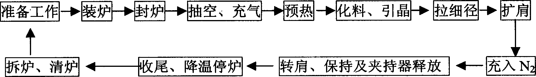
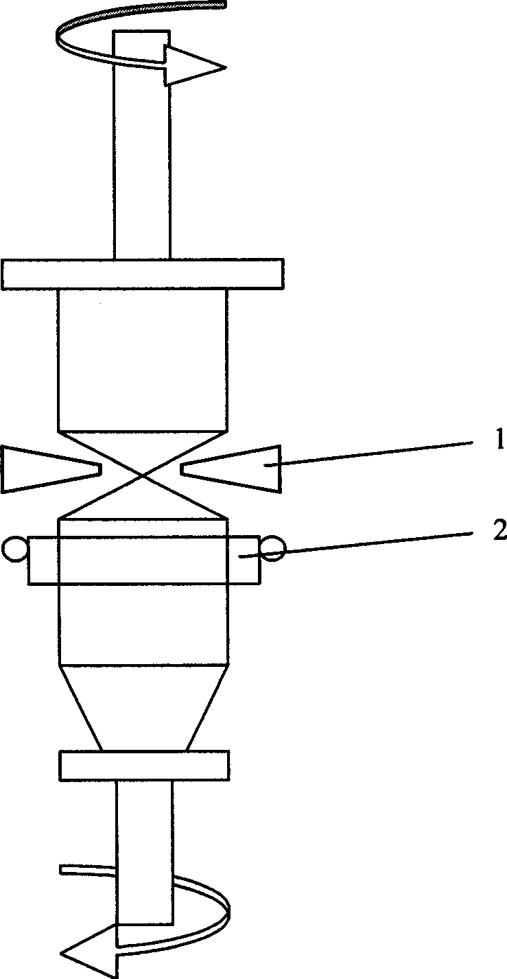
[0014] The production of large-diameter zone-melting silicon single crystals, especially Φ≥4 "zone-melting silicon single crystals, is a test for both the crystal pulling process and the crystal pulling equipment. The zone melting single crystal furnace disclosed in the present invention is produced by the Danish Trust The model is FZ-30 produced by Pusuo Company. During the crystal pulling process, it is necessary to constantly adjust the set point of the generator of the zone melting single crystal furnace, and the set point of the anode voltage of the generator of this equipment is given in percentage. That is, every time the power is adjusted, the percentage will always be displayed on the touch screen. For example, when the diameter of the zone-melted silicon single crystal expands to Φ110mm-130mm, the anode voltage setting point at this time is generally 70%. If the anode voltage is increased by 0.1% , then the set point displayed on the touch screen should be 70.1%.

[...


PUM


Abstract

The invention relates to a silicon single-crystal manufacture method, especially a method to produce major diameter zone melting silicon single-crystal for high-power high voltage, big current semiconductor device. When the diameter of zone melting silicon single-crystal expands to 110mm-130mm, interface turning would happen, adjusting the anode voltage set by zone melting silicon single-crystal furnace generator after an interval of 5-10 seconds and increasing voltage 0.1-0.3%. When the diameter expanding to 110mm, the sporting speed downward the axial is set at the range of 2.0-2.4mm/minute and the rotating speed is set at the range of 4-6 round per minute. In the air pumping and filling process, the hearth pressure should reach 3.0bar-3.2bar, when the diameter expanding to 110mm, the N2 would be filled in and the ratio is 0.5-0.6% compared to Ar. The invention also improves the heat field system of the zone melting silicon single-crystal. Every index of the zone melting silicon single crystal reaches the SEMI standard.

Description

technical field [0001] The invention relates to a method for preparing a silicon single crystal, in particular to a method for preparing a large-diameter zone-melted silicon single crystal for producing high-power, high-voltage, and high-current semiconductor devices. Background technique [0002] As one of semiconductor silicon materials, zone-melted silicon single crystal is mainly used as the main functional material for semiconductor power devices, power integrated devices and semiconductor integrated circuits. With the rapid development of the microelectronics industry, the semiconductor industry has also put forward newer and higher requirements for silicon materials. With the expansion of production scale, semiconductor device manufacturers are gradually requesting to increase the diameter of silicon wafers for the purpose of improving productivity, reducing costs, and increasing profits. Over the years, increasing the diameter of crystals has been an eternal pursuit...

Claims


Application Information

Patent Timeline
Patent Type & Authority Applications(China)
IPC IPC(8): C30B15/00C30B15/20C30B29/06
Inventor 沈浩平刘为钢高福林高树良李翔汪雨田
Owner ZHONGHUAN ADVANCED SEMICON MATERIALS CO LTD
Why Eureka
Try Eureka