Thin film transistor array panel and liquid crystal display

A technology for thin film transistors and liquid crystal displays, which can be used in instruments, nonlinear optics, optics, etc., and can solve problems such as poor visibility and poor twisted nematic liquid crystal displays.

Inactive Publication Date: 2006-02-15
SAMSUNG ELECTRONICS CO LTD
View PDF2 Cites 23 Cited by
  • Summary
  • Abstract
  • Description
  • Claims
  • Application Information

AI Technical Summary

Problems solved by technology

However, this liquid crystal display exhibits poor visibil

Method used


Image

  • Thin film transistor array panel and liquid crystal display
  • Thin film transistor array panel and liquid crystal display
  • Thin film transistor array panel and liquid crystal display

Examples


Embodiment Construction

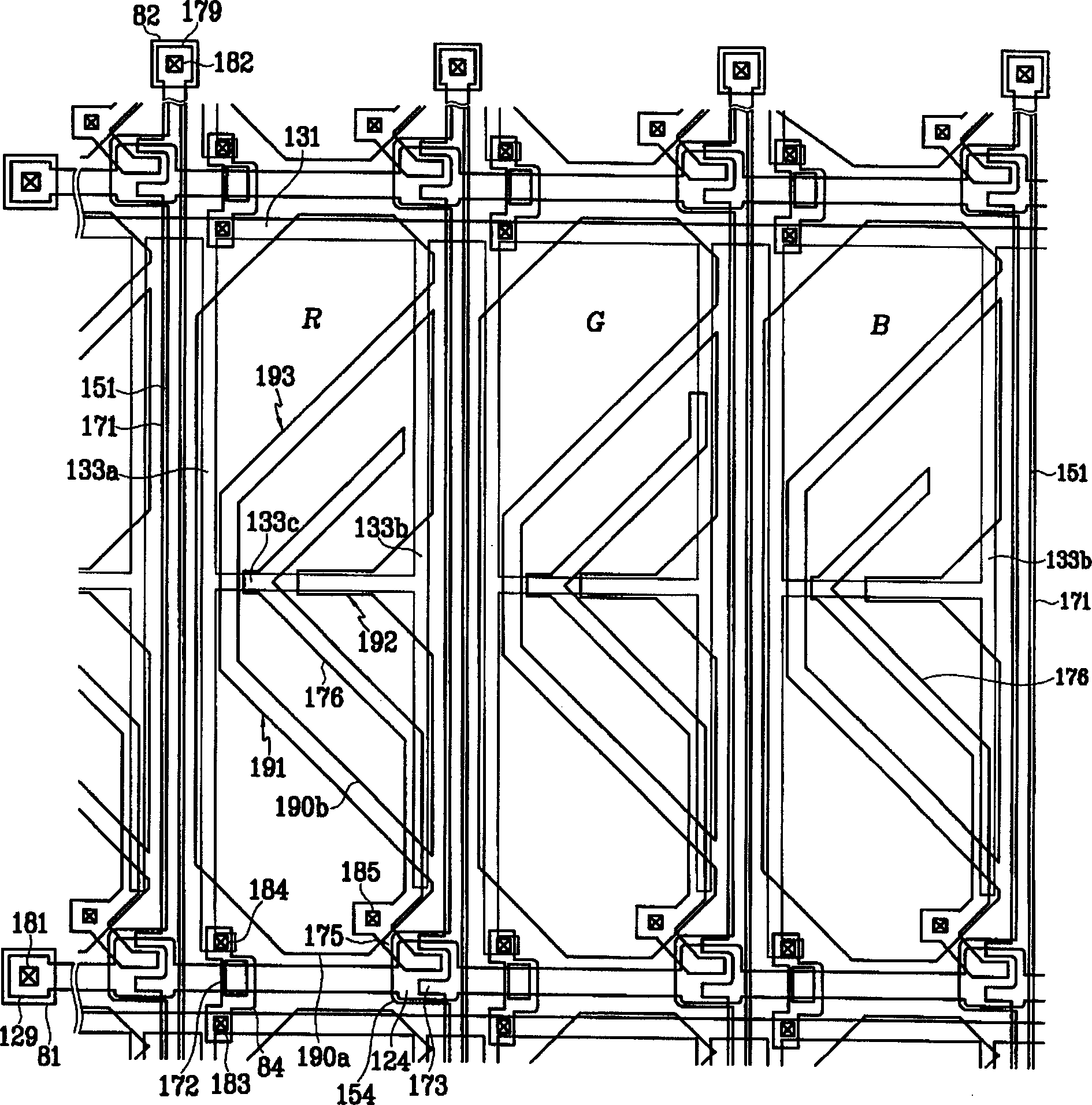
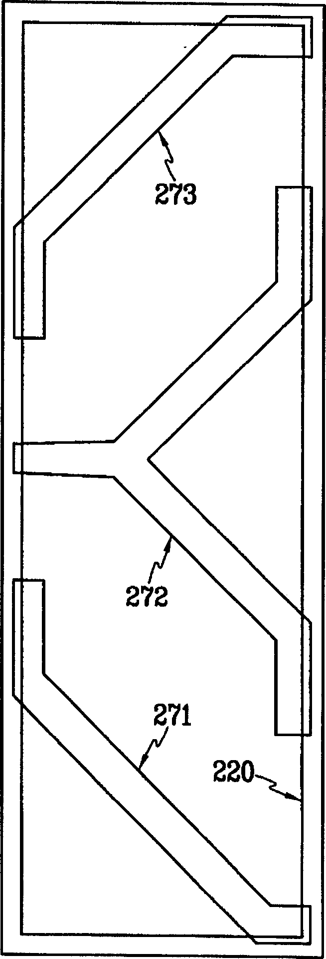
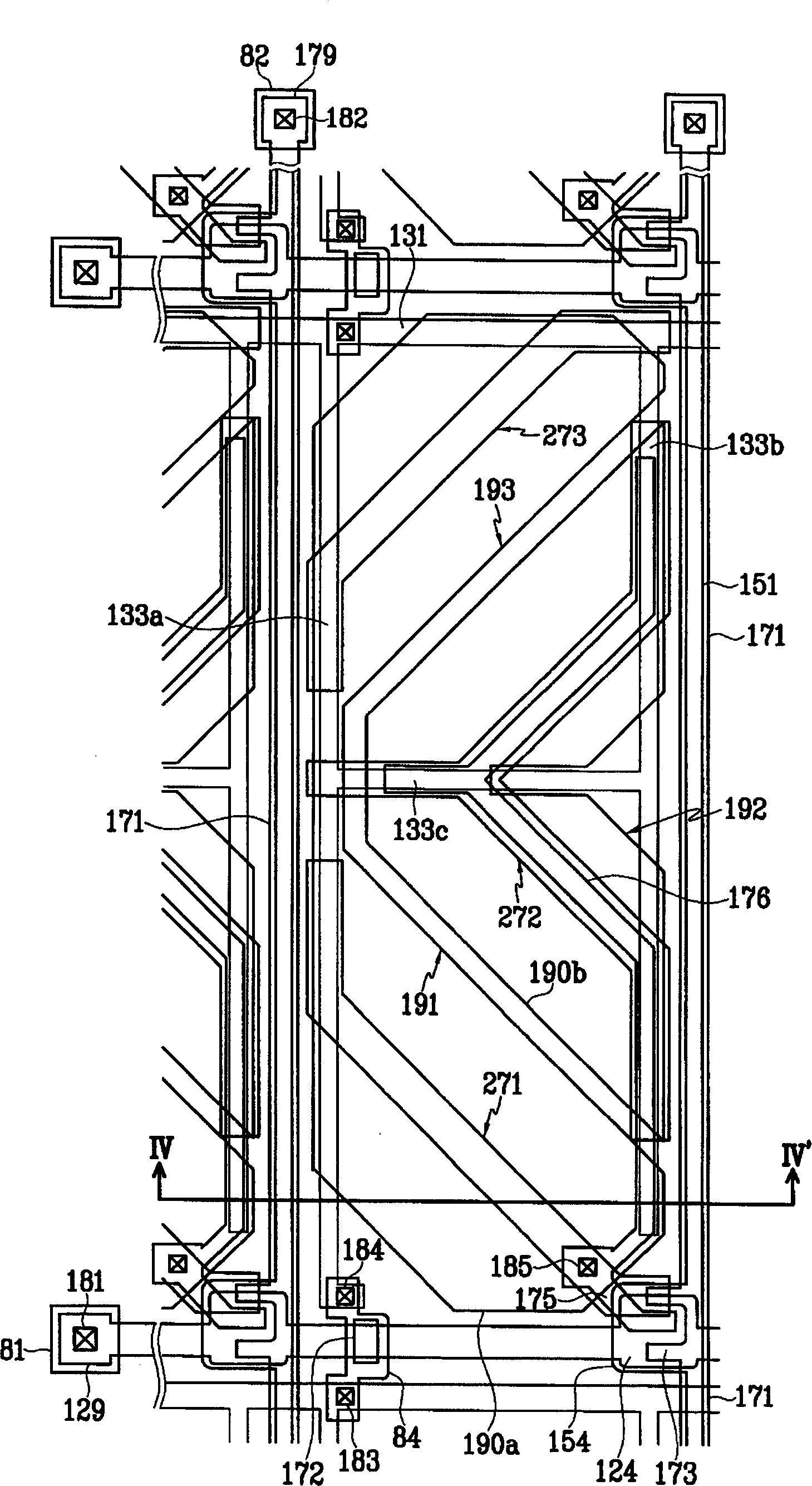
[0031] In order to enable those skilled in the art to practice the present invention, embodiments of the present invention will now be described in detail with reference to the accompanying drawings. However, the present invention can be embodied in different forms, and it is not limited to the embodiments described here.

[0032] In the drawings, the thicknesses and regions of layers are exaggerated for clarity. Where the same reference numerals are attached to the same elements throughout the specification, it should be understood that when a layer, film, region, or substrate is referred to as being "on" another element, it is meant to be directly on the other element. , or there may be other components in between. In contrast, when an element is referred to as being "directly" on other elements, it means that there are no intervening elements.

[0033] Hereinafter, a liquid crystal display and a thin film transistor of a liquid crystal display according to an embodiment o...


PUM


Abstract

The invention provides a LCD including an insulating substrate; a plurality of first signal lines formed on the insulating substrate; a plurality of second signal lines crossing and insulated from the first signal lines; a plurality of thin film transistors (TFT) coupled with the first and second signal lines; and a plurality of pixels including a plurality of first sub-pixel electrodes coupled with the TFTs and a plurality of second sub-pixel electrodes capacitively coupled with the first sub-pixel electrodes, wherein the pixels include a red (R) pixel, a green (G) pixel, and a blue (B) pixel and a voltage ratio or an area ratio of the second sub-pixel electrode with respect to the first sub-pixel electrode is different among the R, G, and B pixels to improve a brightness ratio of R, G, and B components at a lateral position.

Description

[0001] Cross References to Related Applications [0002] This application claims priority to Korean Patent Application No. 10-2004-0061397 filed on Aug. 4, 2004, and Korean Patent Application No. 10-2005-0013458 filed on Feb. 18, 2005, the contents of which are hereby incorporated by reference in their entirety. refer to. technical field [0003] The invention relates to a liquid crystal display and a thin film transistor array panel. Background technique [0004] A liquid crystal display (LCD) is a common type of flat panel display. A liquid crystal display includes two panels provided with field generating electrodes, and a liquid crystal (LC) layer interposed therebetween. The liquid crystal display can display images by applying a voltage to the field generating electrodes to generate an electric field in the liquid crystal layer, which changes the orientation of liquid crystal molecules in the liquid crystal layer to adjust the polarization of incident light. [0005...

Claims


Application Information

Patent Timeline
IPC IPC(8): G02F1/1343G02F1/136
CPCG02F1/133707G02F1/136286G02F1/1368G02F1/133742G02F1/134372
Inventor 严允成损廷昊郑东勋李准宇慎庸桓柳在镇仓学璇金贤昱李昶勋
Owner SAMSUNG ELECTRONICS CO LTD
Why Eureka
Try Eureka