Electronic component, circuit board, electronic apparatus, and method for manufacturing electronic component

A technology for electronic parts and manufacturing methods, applied in the field of manufacturing electronic parts, circuit substrates, electronic instruments and electronic parts, can solve the problems of difficulty in thinning and miniaturization, achieve thinning, improve freedom, and improve The effect of driving electronic components

Inactive Publication Date: 2006-03-22
SEIKO EPSON CORP
View PDF4 Cites 19 Cited by
  • Summary
  • Abstract
  • Description
  • Claims
  • Application Information

AI Technical Summary

Problems solved by technology

On the other hand, in the structure of the above-mentioned Japanese Patent Laid-Open No. 2002-290184, since the SAW element and the integrated circuit are arranged in parallel, it is difficult to miniaturize
Similarly, for the structure of JP

Method used


Image

  • Electronic component, circuit board, electronic apparatus, and method for manufacturing electronic component
  • Electronic component, circuit board, electronic apparatus, and method for manufacturing electronic component
  • Electronic component, circuit board, electronic apparatus, and method for manufacturing electronic component

Examples


Example Embodiment

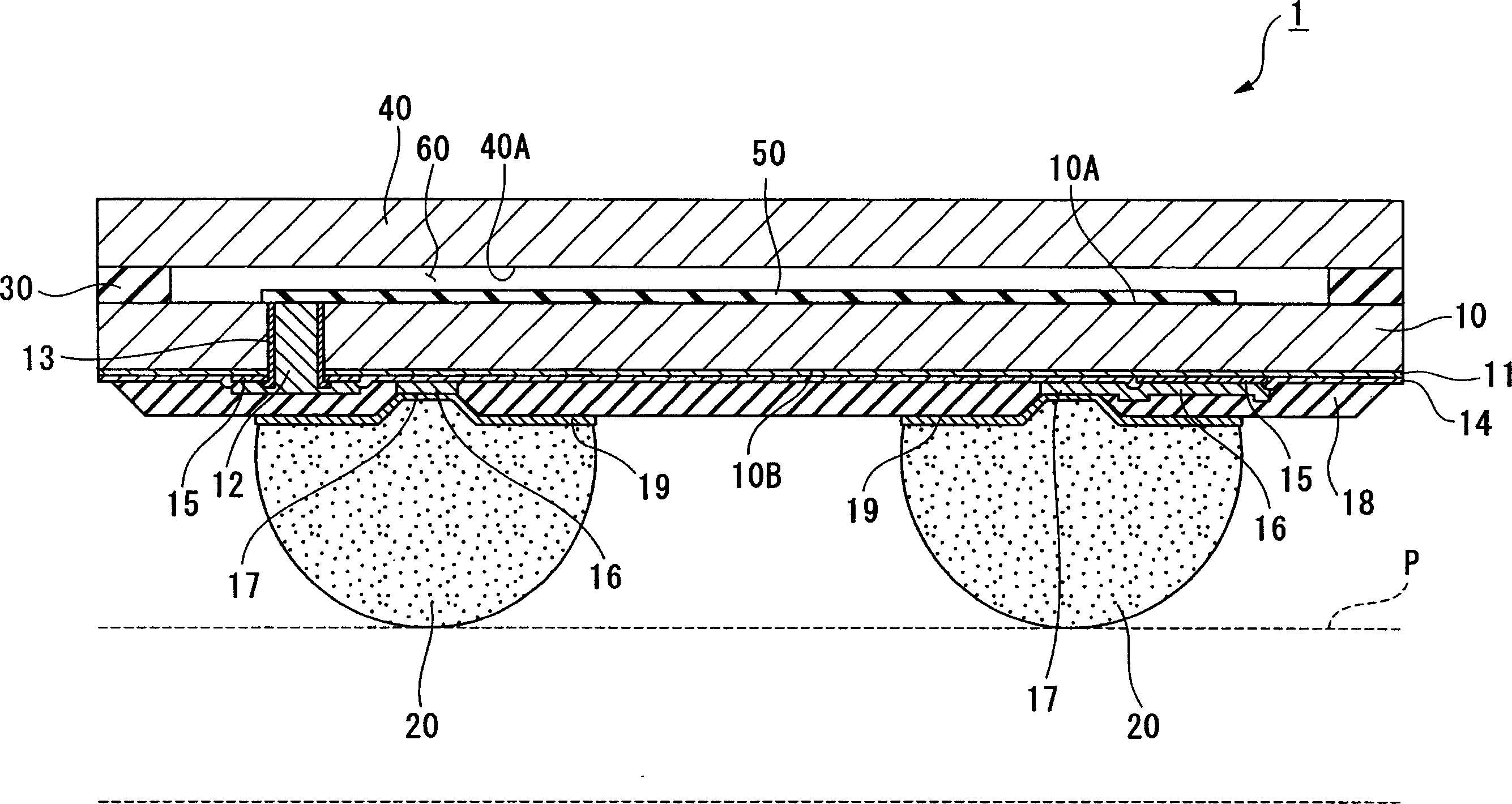
[0052] Refer to the following figure 1 The first embodiment of the electronic component of the present invention will be described. In this embodiment, the case where an electronic component is used in a surface acoustic wave device will be described as an example, and the case where an electronic component is used in a surface acoustic wave device will be described as an example. In the following description, a surface acoustic wave element is appropriately referred to as a "SAW (Surface Acoustic Wave) element" and a surface acoustic wave device is referred to as a "SAW package".

[0053] figure 1 Among them, the SAW package 1 is equipped with: a semiconductor substrate 10 composed of a silicon substrate; a SAW element 50 provided on the first surface 10A side of the semiconductor substrate 10; Penetrating electrode 12 penetrating through surface 10B. The SAW element 50 is provided on the first surface 10A of the semiconductor substrate 10 . The SAW element 50 includes a ...


PUM


Abstract

An electronic component includes: a semiconductor substrate having a first surface and a second surface opposing to the first surface; a trans-substrate conductive plug that penetrates the semiconductor substrate from the first surface to the second surface; an electronic element provided in the vicinity of the first surface of the semiconductor; and a sealing member that seals the electronic element between the sealing member and the first surface, wherein the electronic element is electrically connected to the trans-substrate conductive plug.

Description

technical field [0001] The present invention relates to an electronic component, a circuit substrate, an electronic instrument and a method for manufacturing the electronic component. [0002] This application claims priority from Japanese Patent Application No. 2004-265189 filed on September 13, 2004 and Japanese Patent Application No. 2005-123476 filed on April 21, 2005, the contents of which are incorporated herein by reference. Background technique [0003] In recent years, electronic components including surface acoustic wave elements (hereinafter appropriately referred to as "SAW (Surface Acoustic Wave)" elements) are used in electronic devices such as mobile phones and television receivers. An example of electronic component technology including SAW is disclosed in JP-A-2002-290184 and JP-A-2002-290200. Japanese Patent Laid-Open No. 2002-290184 discloses a packaging technology for electronic components in which a SAW element and an integrated circuit for driving and ...

Claims


Application Information

Patent Timeline
IPC IPC(8): H03H9/25
CPCH01L2224/11
Inventor 伊东春树桥元伸晃
Owner SEIKO EPSON CORP
Why Eureka
Try Eureka