Test fixture in high frequency measuring chip of laser in structure of monocoplanar electrode

A technology of test fixtures and lasers, which is applied in the direction of single semiconductor device testing, semiconductor/solid-state device testing/measurement, etc. It can solve the problems of inaccurate measurement, inability to remove the chip, and damage to the chip that increases the complexity of the measurement.

Inactive Publication Date: 2006-04-19
INST OF SEMICONDUCTORS - CHINESE ACAD OF SCI
View PDF0 Cites 0 Cited by
  • Summary
  • Abstract
  • Description
  • Claims
  • Application Information

AI Technical Summary

Problems solved by technology

[0004] But this method has the following two deficiencies: First, because the chip response measured from the coplanar electrode of the heat sink will include the response of the parasitic elements introduced by the heat sink and the gold wire, and the influence of these parasitic elements is obvious, so the measurement is not accurate enough
In order to obtain the real response of the chip, a series of calibrations are required to deduct the relevant influences on the measurement results, which makes the measurement complicated; secondly, the process of bonding the chip and the gold wire increases the complexity of the measurement and the impact of the chip. The possibility of damage, and once the chip is bonded to the heat sink, it cannot be removed, which has caused great inconvenience to the actual work

Method used


Image

  • Test fixture in high frequency measuring chip of laser in structure of monocoplanar electrode
  • Test fixture in high frequency measuring chip of laser in structure of monocoplanar electrode
  • Test fixture in high frequency measuring chip of laser in structure of monocoplanar electrode

Examples


Embodiment Construction

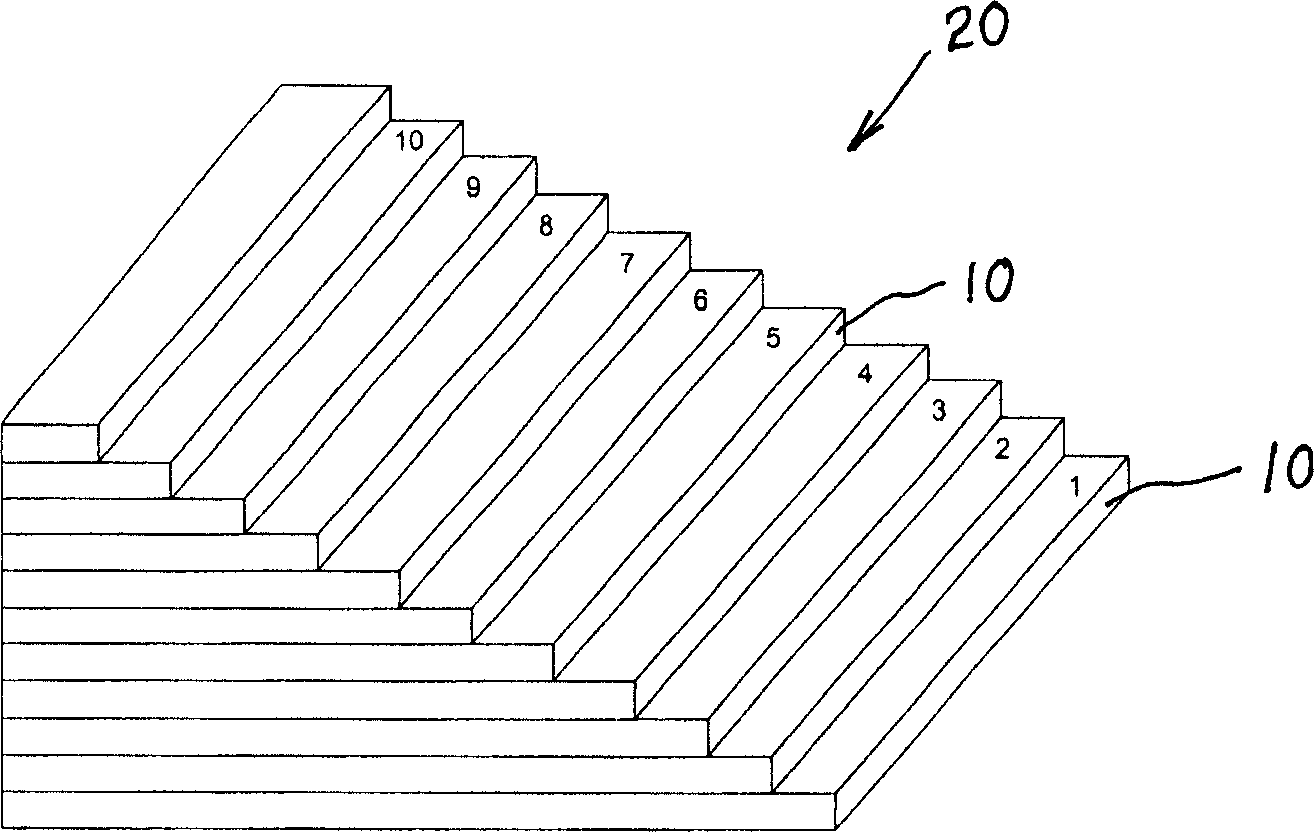
[0021] see figure 1 Shown, a kind of high-frequency test jig of the present invention measures non-coplanar electrode laser chip, comprises:

[0022] A plurality of conductor plates 10, the conductor plates 10 are rectangular, and the plurality of conductor plates 10 are stacked and welded to form a multi-step structure 20; the material of the conductor plates 10 is gold-plated glass ceramics; the multi-step structure 20 is graded from 2 to 15;

[0023] The drop of the multi-step structure 20 is not the same; the multi-step structure 20 with different drop is from small to large or from large to small; the difference between two adjacent steps of the multi-step structure 20 is 5 μm ; Each step surface of the multi-step structure 02 is plated with a metal indium layer, and is made with a corresponding step number.

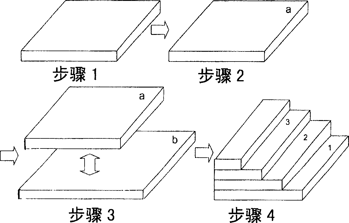
[0024] see figure 2 Shown, the manufacturing schematic diagram of a kind of non-coplanar electrode semiconductor laser test fixture of the present invention, co...


PUM


Abstract

Characters of the test fixture are that: multiple rectangular conductor plates piled to each other are welded to constitute structure of multiple sidesteps; falls in the structure of multiple sidesteps are different to each other.

Description

technical field [0001] The invention belongs to the field of optoelectronic devices, and relates to a fixture for measuring a high-speed semiconductor laser chip of a non-coplanar electrode. Background technique [0002] As a device for generating optical signals, a high-speed light source is one of the most critical components in an optical fiber communication system. High-speed semiconductor lasers are the most important light sources in optical communication systems at present. The high-frequency performance of semiconductor lasers determines the transmission rate of optical communication systems to a certain extent, so it is very important to accurately measure the high-frequency characteristics of semiconductor lasers. [0003] Most of the semiconductor laser chips have a cuboid structure, and the upper and lower surfaces are plated with metal electrodes, corresponding to the P pole and N pole of the laser diode. However, the current commercial high-frequency microwav...

Claims


Application Information

Patent Timeline
Patent Type & Authority Applications(China)
IPC IPC(8): G01R31/26H01L21/66
Inventor 陈诚祝宁华
Owner INST OF SEMICONDUCTORS - CHINESE ACAD OF SCI
Why Eureka
Try Eureka