Semiconductor device and methods of arranging and manufacturing same

A semiconductor and memory technology, which is applied in the field of integrated circuit memory devices and the manufacture of integrated circuit memory devices, and can solve problems such as large chip size

Active Publication Date: 2006-05-31
SAMSUNG ELECTRONICS CO LTD
View PDF1 Cites 18 Cited by
  • Summary
  • Abstract
  • Description
  • Claims
  • Application Information

AI Technical Summary

Problems solved by technology

Thus, when the capacity of the memory cell array (ie, the number of memory cells) increases, the layout area size also increases, which results in a large chip size

Method used


Image

  • Semiconductor device and methods of arranging and manufacturing same
  • Semiconductor device and methods of arranging and manufacturing same
  • Semiconductor device and methods of arranging and manufacturing same

Examples


Embodiment Construction

[0057] The present invention will now be described more fully hereinafter with reference to the accompanying drawings, in which preferred embodiments of the invention are shown. However, this invention may be embodied in different forms and should not be construed as limited to the embodiments set forth herein. Rather, these embodiments are provided so that this disclosure will be thorough and complete, and will fully convey the scope of the invention to those skilled in the art. In the drawings, the thicknesses of layers and regions are exaggerated for clarity. Like numbers refer to like elements throughout the specification.

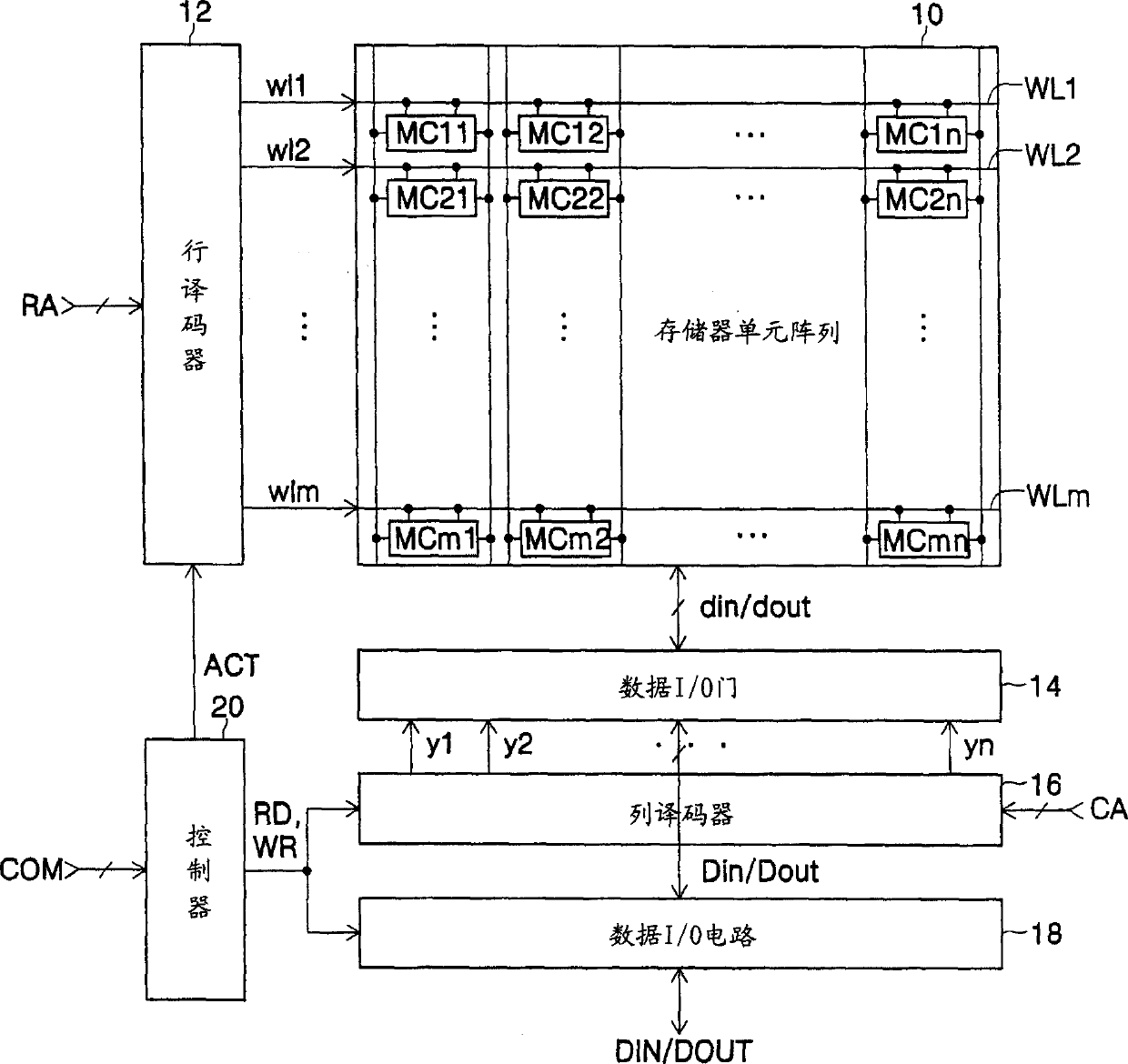
[0058]FIG. 1 is a block diagram illustrating a typical semiconductor memory device. The semiconductor memory device of FIG. 1 includes a memory cell array 10 , a row decoder 12 , a data I / O gate 14 , a column decoder 16 , a data I / O circuit 18 and a controller 20 . In FIG. 1, wl1 to wlm represent word line selection signals, y1 to yn represent colum...


PUM


Abstract

The present invention discloses a semiconductor device and a method for arranging and manufacturing the same. The semiconductor device includes a plurality of inverters including at least one first pull-up transistor and a first pull-down transistor and respectively converting and outputting an input signal; and a plurality of NAND gates including at least two second pull-up transistors and The second pull-down transistor generates an output signal with a high level if at least one of the at least two input signals has a low level, respectively, wherein at least one first pull-up transistor and a first pull-down transistor and at least two second The pull-up transistor and the second pull-down transistor are stacked and arranged on at least two layers.

Description

technical field [0001] The present invention relates to integrated circuit devices, and more particularly to integrated circuit memory devices and methods of manufacturing integrated circuit memory devices. Background technique [0002] A conventional semiconductor memory device includes a memory cell array having a plurality of memory cells storing data and peripheral circuits controlling data input / output to / from the memory cell array. A static memory cell (eg, an SRAM cell) includes a plurality of transistors, and a dynamic memory cell (eg, a DRAM cell) includes a transistor and a capacitor. Peripheral circuits include inverters, NAND gates, and NOR gates, each of which includes a transistor. In typical memory cells and peripheral circuits, multiple transistors are all arranged on the same layer above a semiconductor substrate. Thus, when the capacity of the memory cell array (ie, the number of memory cells) increases, the layout area size also increases, which results ...

Claims


Application Information

Patent Timeline
Patent Type & Authority Applications(China)
IPC IPC(8): H01L27/105G11C7/00G11C11/412G11C11/413H01L21/8239H01L21/8242H01L21/8244H01L27/108H01L27/11
CPCG11C11/412
Inventor 韩公钦南孝润任普托
Owner SAMSUNG ELECTRONICS CO LTD
Why Eureka
Try Eureka