Semiconductor memory system and method for data transmission between memory controller and semiconductor memory

A memory controller, memory system technology, applied in static memory, digital memory information, information storage, etc., can solve the problem that the start and end of data bursts cannot be identified, etc.

Inactive Publication Date: 2006-06-07
INFINEON TECH AG
View PDF0 Cites 0 Cited by
  • Summary
  • Abstract
  • Description
  • Claims
  • Application Information

AI Technical Summary

Problems solved by technology

However, a freely oscillating clock signal brings with it the disadvantage that neither the start nor the end of a data burst can be identified with it
Howeve

Method used


Image

  • Semiconductor memory system and method for data transmission between memory controller and semiconductor memory
  • Semiconductor memory system and method for data transmission between memory controller and semiconductor memory
  • Semiconductor memory system and method for data transmission between memory controller and semiconductor memory

Examples


Embodiment Construction

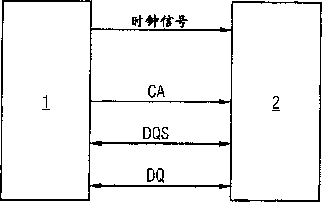
[0023] figure 1 The main components of the semiconductor memory system of the DDR2 generation memory are schematically shown. A clock signal and command / address data CA are transmitted from the memory controller 1 to the semiconductor memory. The bidirectional data strobe signal DQS is transmitted together with the memory data DQ in the semiconductor memory system of the DDR2 generation memory, and notifies the semiconductor memory 2 or the memory controller 1 of the transmission of the memory data DQ to be written or read.

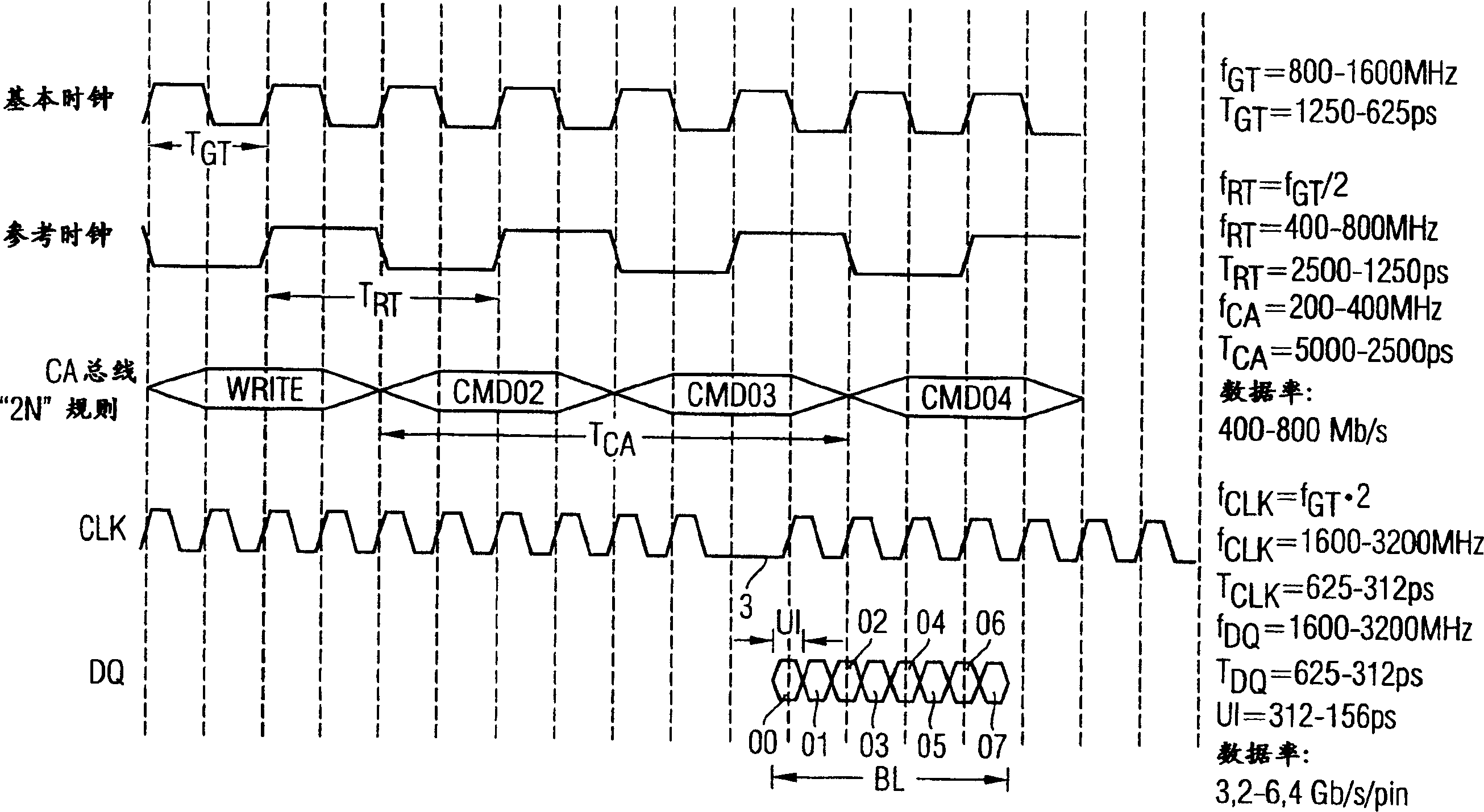
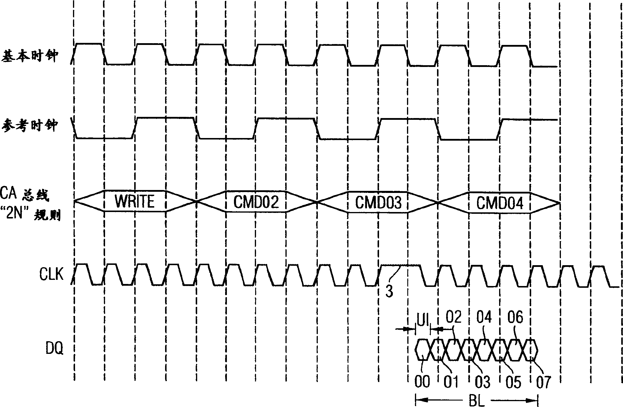
[0024] figure 2 The curve of the signal of the first embodiment is shown schematically with an exemplary signal value range of a future memory of the DDR4 generation, for example. In addition to cycle duration T GT In the range of 1250-625ps (frequency f GT =800-1600MHz) of the basic clock signal, also provided with a cycle duration T RT In the range of 2500-1250p s (frequency f RT = f GT / 2=400-800MHz) reference clock signal. In the clock signal...


PUM


Abstract

A semiconductor memory system is proposed in which the transfer of a burst of memory data (DQ) following the command/address data (CA) of a write/read command (WRITE) is marked with a modified clock signal (CLK). The modified clock signal (CLK) includes an identification region (3, 4) with masked clock edges, so the transfer of memory data (DQ) can be represented by a clock edge following the identification region (3, 4) .

Description

technical field [0001] The invention relates to a semiconductor memory system with a memory controller and a semiconductor memory and to a method for transferring memory data between the memory controller and the semiconductor memory, wherein the transfer of the memory data in bursts is represented by means of a clock signal . Background technique [0002] In future generations of memory, synchronization between instruction / address data (CA) and memory data (DQ) will become increasingly difficult as the length of the unit interval (UI) of bits of memory data (DQ) becomes Less than the expected fluctuation width of the clock signal for command / address data. For example, in the future DDR4 generation memory, it can be expected that the length of the unit interval of the bit of memory data is only 156 ps. Therefore, finding the first memory bit of a data burst that has a time relationship to a read or write command is difficult. The high data transfer rates of future memory ...

Claims


Application Information

Patent Timeline
IPC IPC(8): G11C7/22
CPCG11C7/1051G11C7/1066
Inventor H·鲁克鲍尔
Owner INFINEON TECH AG
Why Eureka
Try Eureka