Semiconductor memory device
A memory and semiconductor technology, applied in the direction of semiconductor devices, static memory, electric solid-state devices, etc., can solve the problems of small tunnel current and large resistance of MTJ components
- Summary
- Abstract
- Description
- Claims
- Application Information
AI Technical Summary
Problems solved by technology
Method used
Image


Examples
no. 1 example
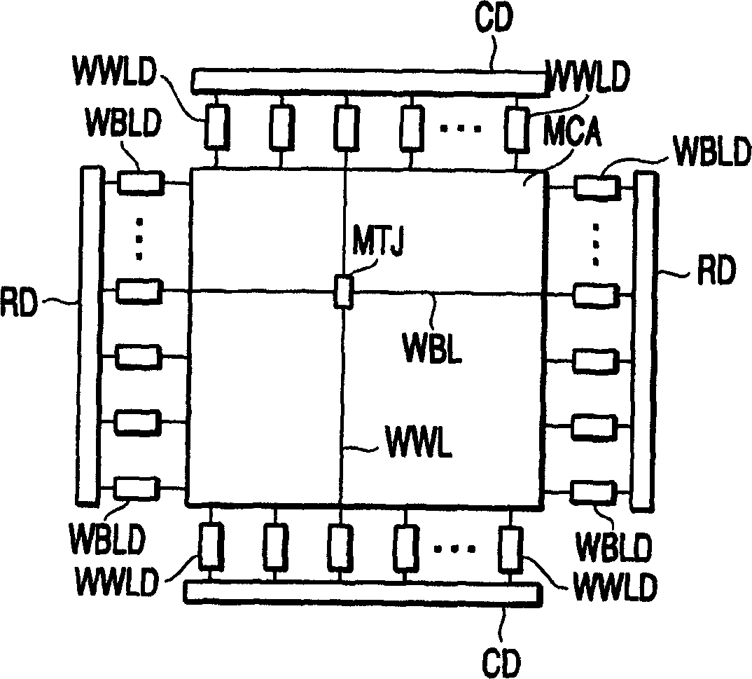
[0046] figure 1 The structure of the semiconductor memory device common to the embodiments of the present invention is schematically shown. figure 1 A memory cell array extracted from a semiconductor memory device and a circuit related to writing are shown. Such as figure 1 As shown, the semiconductor memory device has a memory cell array MCA. As will be discussed in detail later, the memory cell array MCA has a plurality of MTJ elements MTJ, a plurality of write bit lines WBL extending in the x direction (horizontal direction in the drawing), and a plurality of writing bit lines WBL extending in the y direction (vertical direction in the drawing). multiple write word lines WWL. The figure shows only one MTJ element MTJ, one write bit line, and one write word line.
[0047] The MTJ element MTJ may have any structure as long as the MTJ element MTJ can at least store binary data according to a magnetic field applied to the MTJ element MTJ. Such as Figure 58As shown, a str...
no. 2 example
[0068] The second embodiment relates to a method of flowing current through a write line of the semiconductor memory device according to the first embodiment.
[0069] Below, will refer to Figure 8 and 9 , to describe the second embodiment. As an example, the following description corresponds to the figure 2 In the structure of the first embodiment shown, data is written to the MTJ element MTJ located on the left side of the connection line CONWBL. More specifically, as an example of this case, writing is performed on the MTJ element (selected MTJ element) passed by the second write bit line WBL from the top of the drawing.
[0070] Figure 8 and 9 Schematically shows the state of important components during writing according to the second embodiment of the present invention. especially in Figure 8 , the write current flows to the right in the figure through the write bit line (selected write bit line) WBL through the selected MTJ element. exist Figure 9 , the wri...
no. 3 example
[0094] In the third embodiment, in addition to the control of the second embodiment, control is performed so that no current flows in the write line portion adjacent to the selected write line adjacent to the selected MTJ element.
[0095] Figure 12 and 13 Each schematically shows states of important parts of the semiconductor memory device according to the third embodiment during writing. exist Figure 12 , the write current flows to the right in the figure through the selected write bit line WBL. The selected write bit line is the second written bit line from the top of the figure. Figure 12 Corresponds to such as Figure 8 The state of the second embodiment is shown. exist Figure 13 , the write current flows to the left in the figure through the selected write bit line WBL. Figure 13 Corresponds to such as Figure 9 The state of the second embodiment is shown.
[0096] Such as Figure 12 As shown, in the write bit line current circuit connected to the write line...
PUM
 Abstract
Description
Claims
Application Information
 - R&D
- Intellectual Property
- Life Sciences
- Materials
- Tech Scout
- Unparalleled Data Quality
- Higher Quality Content
- 60% Fewer Hallucinations
Browse by: Latest US Patents, China's latest patents, Technical Efficacy Thesaurus, Application Domain, Technology Topic, Popular Technical Reports.
© 2025 PatSnap. All rights reserved.Legal|Privacy policy|Modern Slavery Act Transparency Statement|Sitemap|About US| Contact US: help@patsnap.com