Method for mfg. metal silicified layer

A technology of metal silicide and manufacturing method, which is applied in the field of metal silicide layer and metal silicide layer manufacturing, can solve problems such as spike phenomenon and piping effect, and achieve the effect of solving the spike phenomenon and piping effect and improving the gate area

Active Publication Date: 2006-06-14
UNITED MICROELECTRONICS CORP
View PDF0 Cites 8 Cited by
  • Summary
  • Abstract
  • Description
  • Claims
  • Application Information

AI Technical Summary

Problems solved by technology

[0008] Another object of the present invention is to provide a method for manufacturing a metal silicide layer to solve the spike phenomenon and piping effect caused by nickel silicide in the region heavily doped with P-type or N-type ions

Method used


Image

  • Method for mfg. metal silicified layer
  • Method for mfg. metal silicified layer
  • Method for mfg. metal silicified layer

Examples


Embodiment Construction

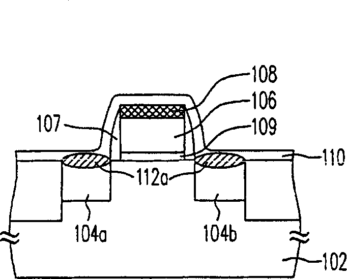
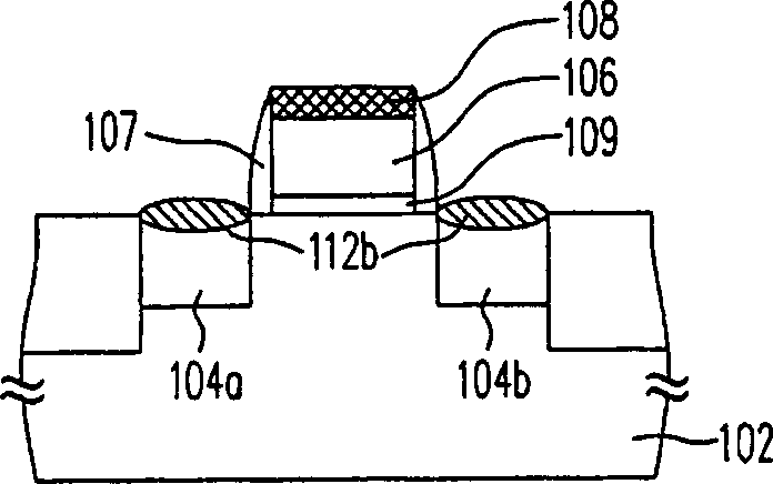
[0017] The concept of the present invention is to form silicide metal layers of different materials on the surface of the substrate, that is, the source region, the drain region and the surface of the gate, so that the problem of small line width and high resistance can be improved at the same time, and the problem of high resistance in the existing process can be solved. Nickel silicide is prone to spiking and piping in the source and drain regions. The following examples are used to illustrate the application of the present invention, but are not intended to limit the scope of the present invention. The present invention can be applied to any steps in the semiconductor process that require simultaneous formation of metal silicides on materials with different crystal structures.

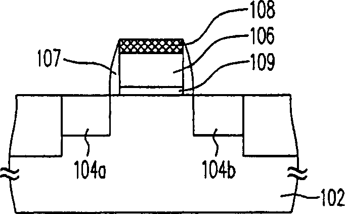
[0018] Figure 1A to Figure 1E It shows a sectional view of the manufacturing process of a metal silicide layer according to a preferred embodiment of the present invention.

[0019] First, please r...


PUM


Abstract

The invention is a method for manufacturing metallic silicide layer, forming at least a grid on a substrate, then forming a hard mask on the grid surface and exposing the substrate surface, then forming a first metallic silicide layer on the exposed substrate surface, where the first metallic silicide layer is made of one of the cobalt silicide and Ti silicide, successively removing the hard mask and forming a second metallic silicide layer on the grid surface, where the second metallic silicide layer is selected from one of the nickel silicide, Pt silicide, Pd silicide and nickel alloy. The invention can improve the problem of small line width and high resistance and solve the problems of peak phenomenon and surging in the source and drain regions caused by nickel silicide.

Description

technical field [0001] The invention relates to a semiconductor process method and structure, in particular to a method for manufacturing a metal silicide layer, which is used to form metal silicide layers of different materials on substrates with different crystal structures. Background technique [0002] In the VLSI trend, the size of semiconductor components is continuously reduced and the integration level is continuously improved. By shrinking the size of electronic components, semiconductor integrated circuits can be completed with maximum integration capabilities. However, as the size of electronic components shrinks, many challenges arise in the fabrication of integrated circuits. Especially as the appearance of components continues to shrink, the need to reduce the resistance of the electrical connection structure is more important than ever, because the increase in resistance will cause the operation speed of the device to slow down due to the delay of capacitance...

Claims


Application Information

Patent Timeline
Patent Type & Authority Applications(China)
IPC IPC(8): H01L21/3205H01L21/283H01L21/314H01L21/321
Inventor 陈意维洪宗佑江怡颖谢朝景张毓蓝
Owner UNITED MICROELECTRONICS CORP
Why Eureka
Try Eureka