
Electro-optical device, image printing apparatus, and method of manufacturing electro-optical device

An electro-optical device and electro-optic technology, applied to the equipment of the electric recording process using the charge pattern, the electric recording process using the charge pattern, optics, etc., can solve the problem of poor light utilization efficiency

Inactive Publication Date: 2006-07-19
SEIKO EPSON CORP
View PDF2 Cites 6 Cited by
  • Summary
  • Abstract
  • Description
  • Claims
  • Application Information

AI Technical Summary

Problems solved by technology

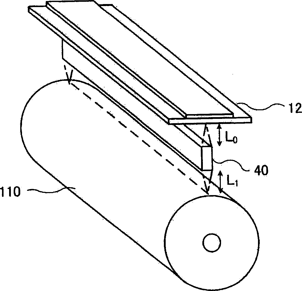
[0007] However, since there is an operating distance L between the light entrance of the focusing lens array 40 and the EL element array, o The space of approximately equal distance, that is, the air layer, so there is light that does not enter the focusing lens array 40 in the light emitted from the EL element.
That is, there is a problem that the utilization efficiency of light is poor

Method used


Image

  • Electro-optical device, image printing apparatus, and method of manufacturing electro-optical device
  • Electro-optical device, image printing apparatus, and method of manufacturing electro-optical device
  • Electro-optical device, image printing apparatus, and method of manufacturing electro-optical device

Examples


Embodiment Construction

[0055]

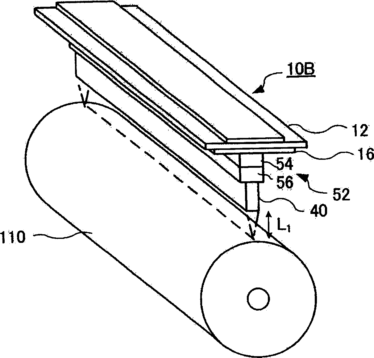
[0056] figure 2 It is a schematic perspective view showing an electro-optical device 10B according to an embodiment of the present invention. The illustrated electro-optical device 10B is used as an image carrier (such as figure 2 A linear optical head for writing a latent image in the shown photosensitive drum 110). The electro-optical device 10B includes a light-emitting panel (electro-optical panel) 12 in which a plurality of organic EL elements (electro-optical elements) are arranged on the same plane, and a focusing lens array 40 superimposed on the light-emitting panel 12 . Between the light-emitting panel 12 and the focusing lens array 40 is interposed a light-transmissive spacer 52 made of glass or plastic, and the spacer 52 has a plurality of light-transmissive spacers 56 and 58 laminated. The focusing lens array 40 is disposed between the light emitting panel 12 on which the EL element array is provided and the photosensitive drum 110 . The light from...


PUM


Abstract

An electro-optical device includes an electro-optical panel which has a plurality of electro-optical elements whose light-emitting characteristics or transmissive characteristics are changed by electrical energy applied; a converging lens array which has a plurality of distributed index lenses, each transmitting light traveling in the electro-optical panel to form an erect image with respect to an image on the electro-optical panel, the images formed by the plurality of distributed index lenses constituting a continuous image; and a transmissive spacer unit which is provided between the electro-optical panel and the converging lens array so as to be bonded to them. The spacer unit includes a laminated structure of a plurality of transmissive spacer members.

Description

technical field [0001] The present invention relates to an electro-optical device including an electro-optical panel on which electro-optical elements such as light-emitting elements and light valve elements are arranged, an image printing apparatus using the electro-optical device, and a method of manufacturing the electro-optical device. Background technique [0002] In order to write an electrostatic latent image on an image carrier (such as a photosensitive drum) of an electrophotographic image printing apparatus, an array using electroluminescence elements (hereinafter referred to as 'EL elements') has been developed. In this technique, a focusing lens array is generally arranged between the EL element array and the image carrier (for example, refer to Patent Document 1 and Patent Document 2). Figure 7 ). As the focusing lens array, there is, for example, SLA (Self-focusing Lens Array) available from Nippon Panglass Co., Ltd. (Self-focus \SELFOC is a registered tradema...

Claims


Application Information

Patent Timeline
Patent Type & Authority Applications(China)
IPC IPC(8): G03G15/04G03G15/08G03G15/00
Inventor 植松弘一
Owner SEIKO EPSON CORP
Learn More