Display apparatus

A technology for display devices and display pixels, applied in identification devices, static indicators, optics, etc., can solve problems such as unsatisfactory and incapable of manufacturing liquid crystal display devices with display performance

Inactive Publication Date: 2006-08-09
TOSHIBA MATSUSHITA DISPLAY TECH
View PDF0 Cites 5 Cited by
  • Summary
  • Abstract
  • Description
  • Claims
  • Application Information

AI Technical Summary

Problems solved by technology

[0006] However, even with such a manufacturing method, it cannot meet the thinner and lighter requirements of the market.
In addition, with...

Method used


Image

  • Display apparatus
  • Display apparatus
  • Display apparatus

Examples


Embodiment Construction

[0040] A display device according to an embodiment of the present invention will be described below with reference to the drawings.

[0041] (first embodiment)

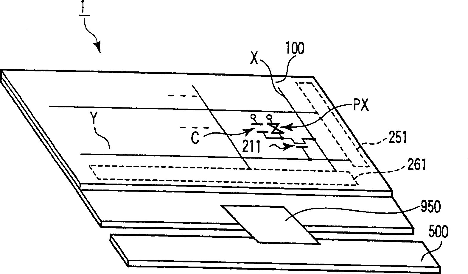
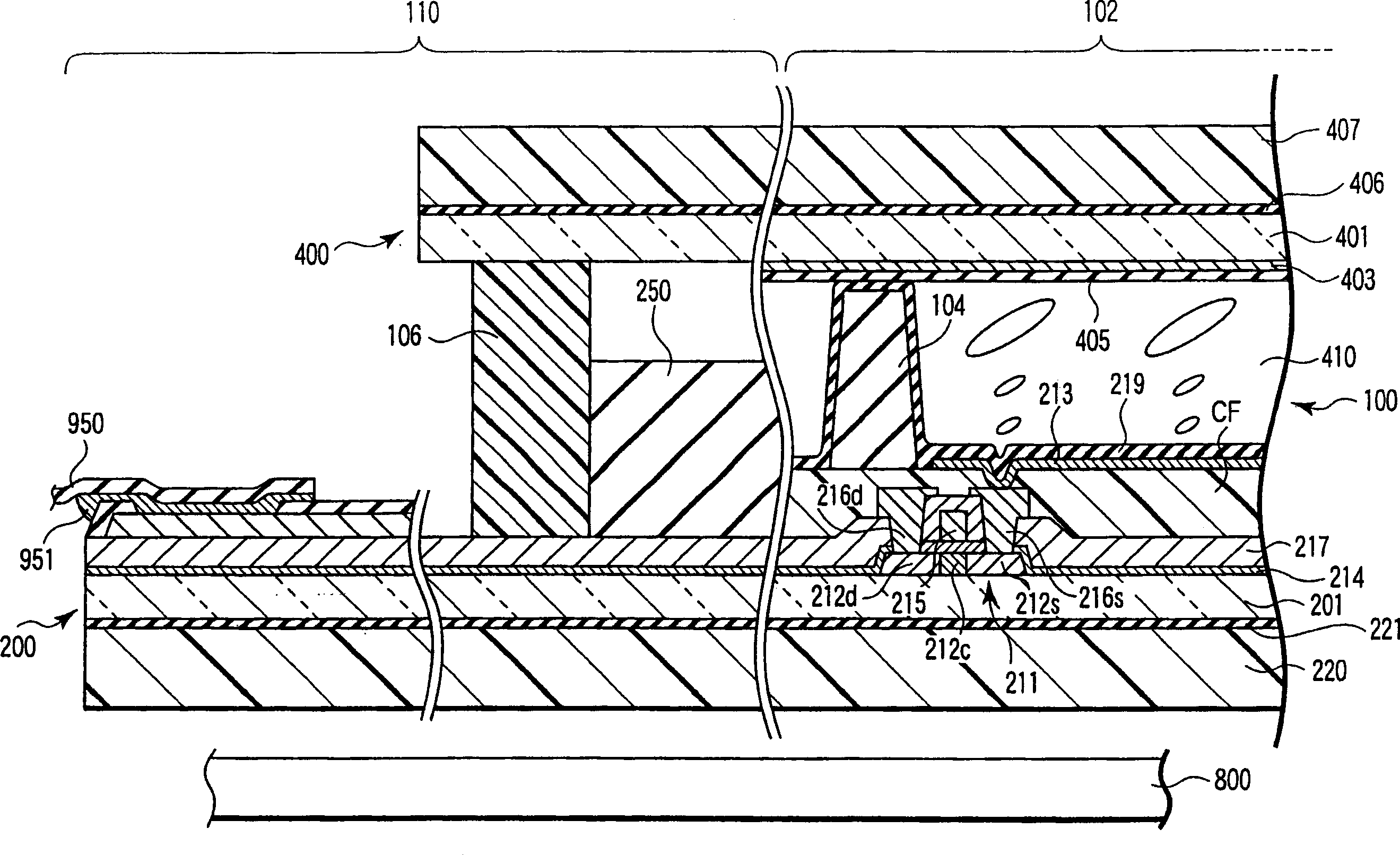
[0042] like figure 1 and figure 2 As shown, the liquid crystal display device 1, which is the display device according to the first embodiment, has a light-transmissive liquid crystal panel 100, a drive circuit board 500 for supplying drive signals to the liquid crystal panel 100, and a backlight for illuminating the liquid crystal panel 100 from the back side. source unit 800. The liquid crystal panel 100 and the driving circuit substrate 500 are connected through the flexible wiring substrate 950 . The flexible wiring substrate 950 is electrically connected to the liquid crystal panel 100 and the driving circuit substrate 500 through an anisotropic conductive film (ACF) 951 .

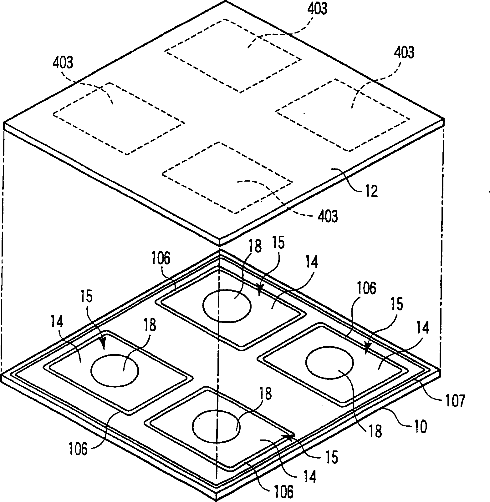
[0043] The liquid crystal panel 100 has a diagonal 12.1-inch effective display area 102 including a plurality of display pixel portions...


PUM

PropertyMeasurementUnit
Thicknessaaaaaaaaaa

Abstract

A display apparatus with a plurality of display pixel sections includes glass substrate, which are formed to have a thickness that permits bending of the display apparatus, and polarizer plates, which are disposed on the glass substrates, respectively. The polarizer plates are thicker than the glass substrates.

Description

[0001] This application is a divisional application of the parent application with the title of invention "display device and its manufacturing method", the filing date is January 20, 2004, and the application number is 03800714.2 (PCT / JP 03 / 06071). technical field [0002] The present invention relates to a display device and a manufacturing method thereof, in particular to a structure of a display device capable of achieving thinning. Background technique [0003] Flat panel display devices represented by liquid crystal display devices take full advantage of the characteristics of light weight, thin thickness and low power consumption, and are applied in various fields. Among them, liquid crystal display devices are mostly used in portable information devices represented by personal computers. [0004] In recent years, further thinning of such liquid crystal display devices has been demanded. In order to meet such requirements, the use of off-duty glass substrates of less...

Claims


Application Information

Patent Timeline
IPC IPC(8): G02F1/1335G02F1/133G02F1/136G09G3/36G09F9/00
Inventor 木下正树川又健司山中训栗须宏之宫崎达哉川田靖
Owner TOSHIBA MATSUSHITA DISPLAY TECH
Why Eureka
Try Eureka