

Semiconductor device and method for manufacturing it
一种制造方法、半导体的技术,应用在半导体/固态器件制造、半导体器件、电气元件等方向,能够解决偏压温度不稳定等问题
- Summary
- Abstract
- Description
- Claims
- Application Information
AI Technical Summary
Problems solved by technology
Method used
Image

Examples
Embodiment Construction
[0045] In order to make the above-mentioned purposes, features and advantages of the present invention more obvious and understandable, the preferred embodiments are specifically cited below, together with the accompanying drawings, and are described in detail as follows:
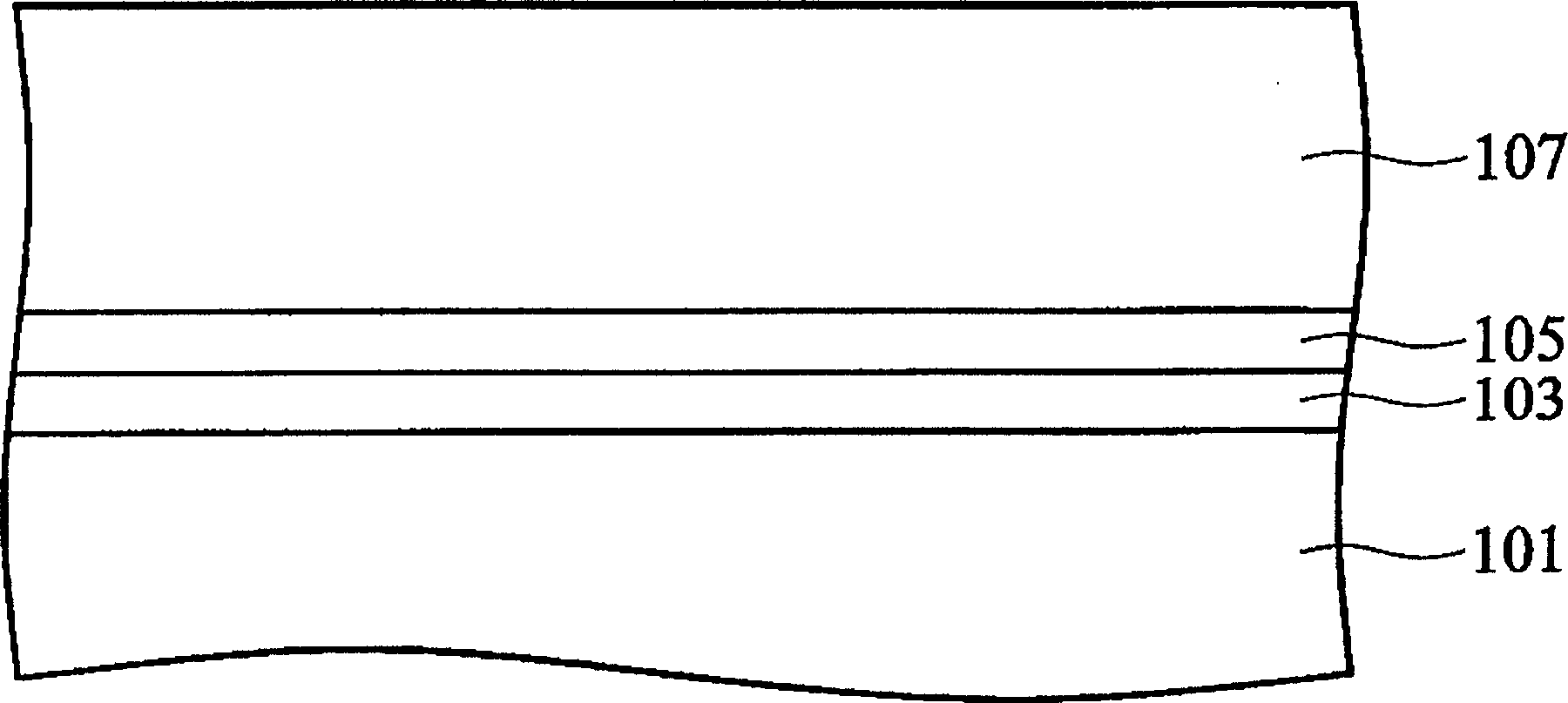
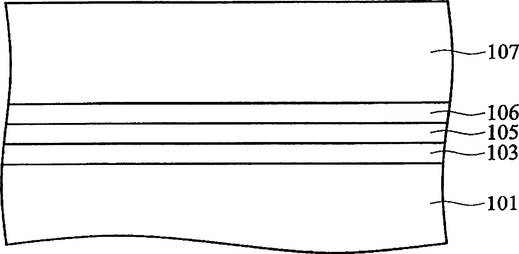
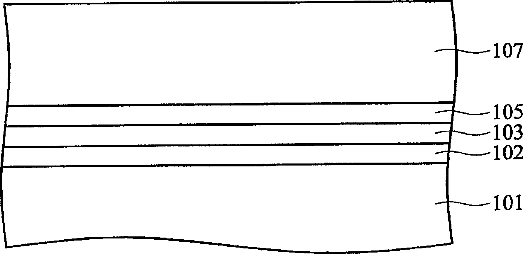
[0046] figure 1 What is shown is a cross-sectional view of an integrated circuit in a manufacturing process. The drawings are for illustration purposes only and are not drawn to scale. Wherein, the semiconductor substrate 101 is preferably a silicon wafer, but may also include Ge, SiGe, strained silicon (strained silicon), strained germanium (strained germanium), GaAs, silicon insulator (siliconon insulator, SOI), germanium-covered insulator (germanium on insulator, GOI), a combination of the above materials, or a multi-layer stack structure such as Si / SiGe.
[0047] The first nitrogen-containing layer 103 can be deposited by jet vapor deposition (JVD) method. In a preferred embodiment, the thickness of t...
PUM
| Property | Measurement | Unit |
|---|---|---|
| uniformity index | aaaaa | aaaaa |
| deposition rate | aaaaa | aaaaa |
Abstract
Description
Claims
Application Information