Memory outputting circuit and data outputting method

An output-level circuit and memory technology, applied in static memory, digital memory information, information storage, etc., can solve problems affecting SRAM read time, output delay, etc.

Active Publication Date: 2006-08-16
VIA TECH INC
View PDF0 Cites 12 Cited by
  • Summary
  • Abstract
  • Description
  • Claims
  • Application Information

AI Technical Summary

Problems solved by technology

Since thousands of SRAM cells in the SRAM are coupled to the output stage circuit, a large amount of parasitic capacitance is coupled to the output stage circuit. S

Method used


Image

  • Memory outputting circuit and data outputting method
  • Memory outputting circuit and data outputting method
  • Memory outputting circuit and data outputting method

Examples


Embodiment Construction

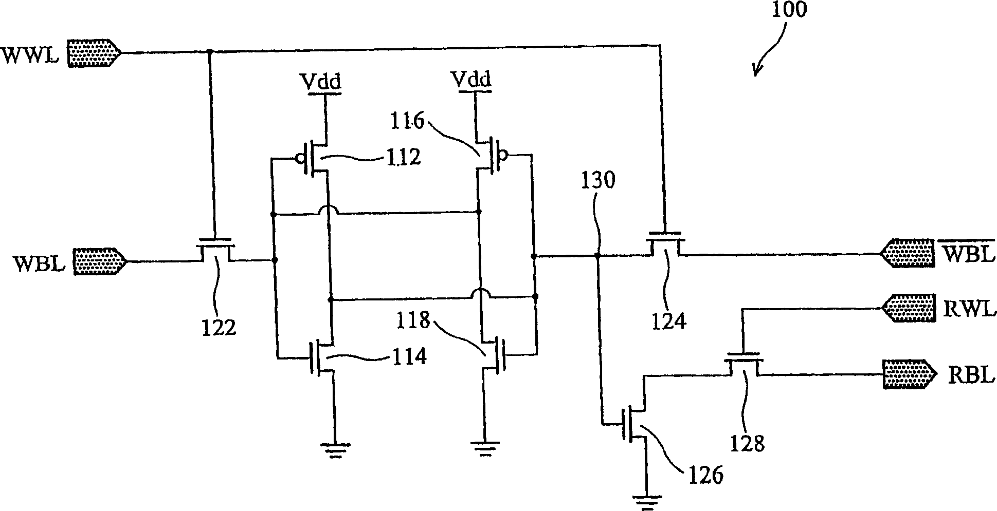
[0047] figure 1 is a circuit diagram of a SRAM cell 100 . The SRAM unit 100 is a dual port 8-transistor (8T) memory unit with a single output terminal. The eight transistors include pull-up transistors 112 and 116 , pull-down transistors 114 and 118 , pass gate transistors 122 and 124 , and sense port transistors 126 and 128 . The pull-up transistors 112 and 116 are PMOS transistors, and the pull-down transistors 114 and 118 , pass gate transistors 122 and 124 , and sense port transistors 126 and 128 are NMOS transistors. However, the present invention still allows other configurations of NMOS and PMOS transistors.

[0048] The sources of the pull-up transistors 112 and 116 are coupled to the voltage source Vdd. The drain of the pull-up transistor 112 is coupled to the source of the pass-gate transistor 124 , the drain of the pull-down transistor 114 , and the gate of the pull-up transistor 116 . Likewise, the drain of pull-up transistor 116 is coupled to the source of pas...


PUM


Abstract

A memorizer output stage circuit, including: the first pre-charging circuit, couple with the reading position line, the reading position line couple with the output end of some memorizer units, the first pre-charging circuit charge the reading position line to high electric potential before read some memorizers at the some level; the sensing amplifier couple with the reading position line, use to test the pressure of the reading position line, and output the result signal to the two output nodes after comparing with the high electric potential.

Description

technical field [0001] The present invention relates to an output stage circuit of a memory, in particular to an output stage circuit of a static random access memory (static random access memory, SRAM). Background technique [0002] In the memory, the data is mostly binary bits, and each bit needs a circuit unit responsible for storing its state as 0 or 1. This circuit unit is called a storage unit, and they are arranged in a rectangular array to form the main body of the memory. In the memory, the selected memory cells can be determined by the output signal of the control circuit to write and read data. When writing, the memory cell can be selected through the input and output selection circuit, and then the bit to be written is stored in the memory cell. On the contrary, when reading, the memory cell can be selected through the input and output selection circuit, and the stored bit state can be sent out through the output stage circuit in the form of current or voltage. ...

Claims


Application Information

Patent Timeline
IPC IPC(8): G11C11/417G11C11/419G11C7/10G11C7/12
Inventor 黄超圣
Owner VIA TECH INC
Why Eureka
Try Eureka