Image sensor for semiconductor light-sensing device and image processing apparatus using the same

一种图像处理装置、图像传感器的技术,应用在半导体器件、固体图像信号发生器、电固体器件等方向,能够解决固定图像噪声误差、占据、不能提取颜色信息等问题

Inactive Publication Date: 2006-11-29
SAMSUNG ELECTRO MECHANICS CO LTD
View PDF0 Cites 11 Cited by
  • Summary
  • Abstract
  • Description
  • Claims
  • Application Information

AI Technical Summary

Problems solved by technology

In this case, if the red R and blue B signals are distorted by noise, an error such as fixed image noise occurs in the CMOS image sensor
Also, if white and dark noise dominate due to lack of consistency in the manufacturing process, interpolation becomes less precise due to fixed image noise, which makes it impossible to extract accurate color information for each pixel

Method used


Image

  • Image sensor for semiconductor light-sensing device and image processing apparatus using the same
  • Image sensor for semiconductor light-sensing device and image processing apparatus using the same
  • Image sensor for semiconductor light-sensing device and image processing apparatus using the same

Examples


Embodiment Construction

[0066] Preferred embodiments according to the present invention will now be described in detail with reference to the accompanying drawings. Components having substantially the same function and configuration will be denoted by the same reference numerals.

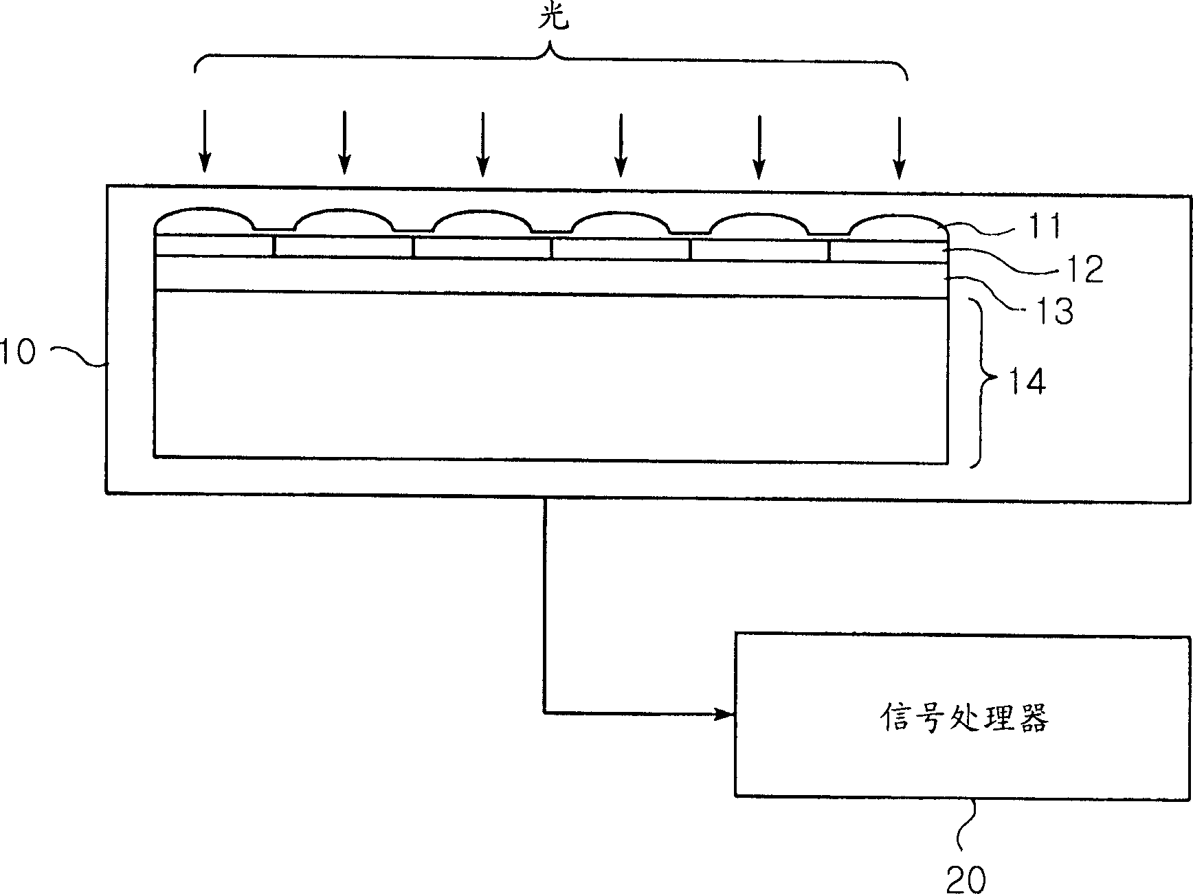
[0067] Figure 5 is a block diagram of an image processing device according to the present invention.

[0068] refer to Figure 5 , The image processing apparatus according to the present invention includes: an image sensor (IMS) for sensing light from an image of an object; and a signal processor 500 for processing a signal from the IMS.

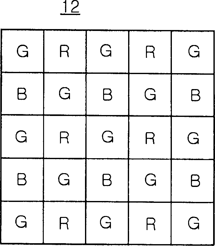
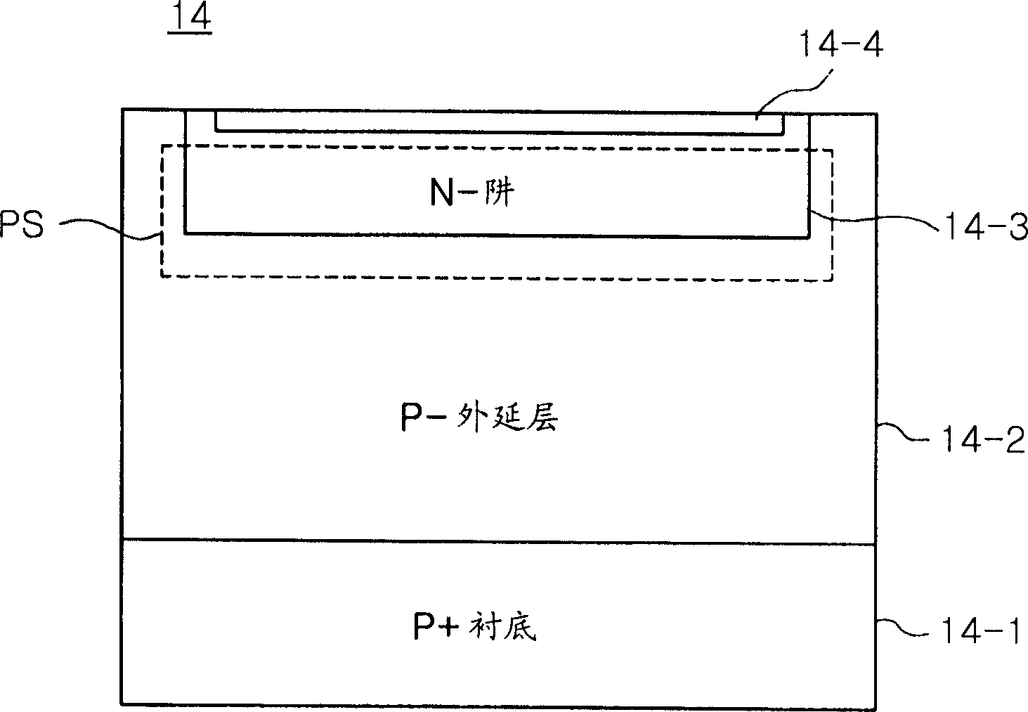
[0069] refer to Figure 5 , the IMS includes: a lens array 100, a color filter array 200, a protective layer 300, and a pixel sensor array 400, each formed in a silicon semiconductor. The lens array 100 includes a plurality of microlenses 110 formed in a two-dimensional matrix. Here, each microlens focuses incident light to a predetermined area.

[0070] Figure 6 is showing Figure...


PUM


Abstract

The invention relates to an image sensor and an image processing apparatus using the same having a color filter array with open window cells alternating with single color filter cells. The image sensor includes a lens array containing a plurality of microlenses, a color filter array having a plurality of open window cells and color filter cells, each corresponding to each microlens. The image sensor also includes a protection layer, and a pixel sensor array having a first photosensor sensing a first light passed through each color filter cell, a second photosensor formed under the first photosensor, sensing a second light passed through each color filter cell, a third photosensor sensing a third light passed through each open window cell, and a fourth photosensor formed under the third photosensor, sensing a fourth light passed through each open window cell.

Description

[0001] This application claims priority from Korean Patent Application No. 2005-44149 filed in the Korean Intellectual Property Office on May 25, 2005, the entire contents of which are hereby incorporated by reference. technical field [0002] The present invention relates to image sensors and image processing devices used in video cameras, digital still cameras, and the like. More particularly, the present invention relates to an image sensor for a semiconductor photosensitive device using a color filter array having open windows and monochromatic color filters alternated with each other, and an image processing apparatus using the same for Multiple color information is used per pixel to enable more precise interpolation, which is used to extract more precise colors per pixel. Background technique [0003] In general, recent developments in image communication by means of wired / wireless high-speed network systems, and image input and recognition technologies such as those u...

Claims


Application Information

Patent Timeline
Patent Type & Authority Applications(China)
IPC IPC(8): H01L27/146G02B5/00H04N5/335H01L27/14H04N9/07
CPCH01L27/14647H01L27/14621H01L27/14627H01L31/02162H04N9/045H04N2209/047H04N25/134H01L27/146
Inventor 姜信在崔愿太高主烈朴得熙
Owner SAMSUNG ELECTRO MECHANICS CO LTD
Why Eureka
Try Eureka