Image sensor for semiconductor light-sensing device and image processing apparatus using the same

a technology of image processing apparatus and light-sensing device, which is applied in the direction of optical radiation measurement, radiation control device, instruments, etc., can solve the problems of less accurate interpolation, degeneration of voltage signal, and more severe effects, so as to minimize the effect of defective pixels or noise, more accurate interpolation, and more accurate color for each pixel

Inactive Publication Date: 2008-03-25
SAMSUNG ELECTRO MECHANICS CO LTD
View PDF5 Cites 2 Cited by
  • Summary
  • Abstract
  • Description
  • Claims
  • Application Information

AI Technical Summary

Benefits of technology

[0028]The present invention has been made to solve the foregoing problems of the prior art and it is therefore an object of the present invention to provide an image sensor for semiconductor light-sensing device which uses a color filter array having open window cells alternating with single color filter cells to allow using information of a plurality of colors for each pixel during interpolation, minimizing the effects from defective pixels or noise to enable more accurate interpolation, thereby extracting more accurate color for each pixel and an image processing apparatus using the same.
[0034]The pixel sensor array further includes a P+ shallow junction layer made of P+ semiconductor material in a predetermined third depth from the upper surface of the epitaxial layer in order to prevent any surface defects of the epitaxial layer.

Problems solved by technology

At this point, the voltage signal may be degenerated due to noise, which indicates mediocre characteristics against noise.
Thus, if the red R and blue B signals are distorted by noise in this case, this may be a cause for an error in the CMOS image sensor such as the fixed pattern noise.
That is, if white and dark noises take up large portions in red and blue signals due to lack of uniformity in the manufacturing process, the interpolation becomes less accurate due to the fixed pattern noise.
This is more severe in the case of highly dense pixel arrangement with small pixels.

Method used


Image

  • Image sensor for semiconductor light-sensing device and image processing apparatus using the same
  • Image sensor for semiconductor light-sensing device and image processing apparatus using the same
  • Image sensor for semiconductor light-sensing device and image processing apparatus using the same

Examples


Embodiment Construction

[0053]Preferred embodiments of the present invention will now be described in detail with reference to the accompanying drawings. The constituent parts having substantially the same functions and constitutions will be denoted by the same reference numerals.

[0054]FIG. 5 is a block diagram of an image processing apparatus according to the present invention.

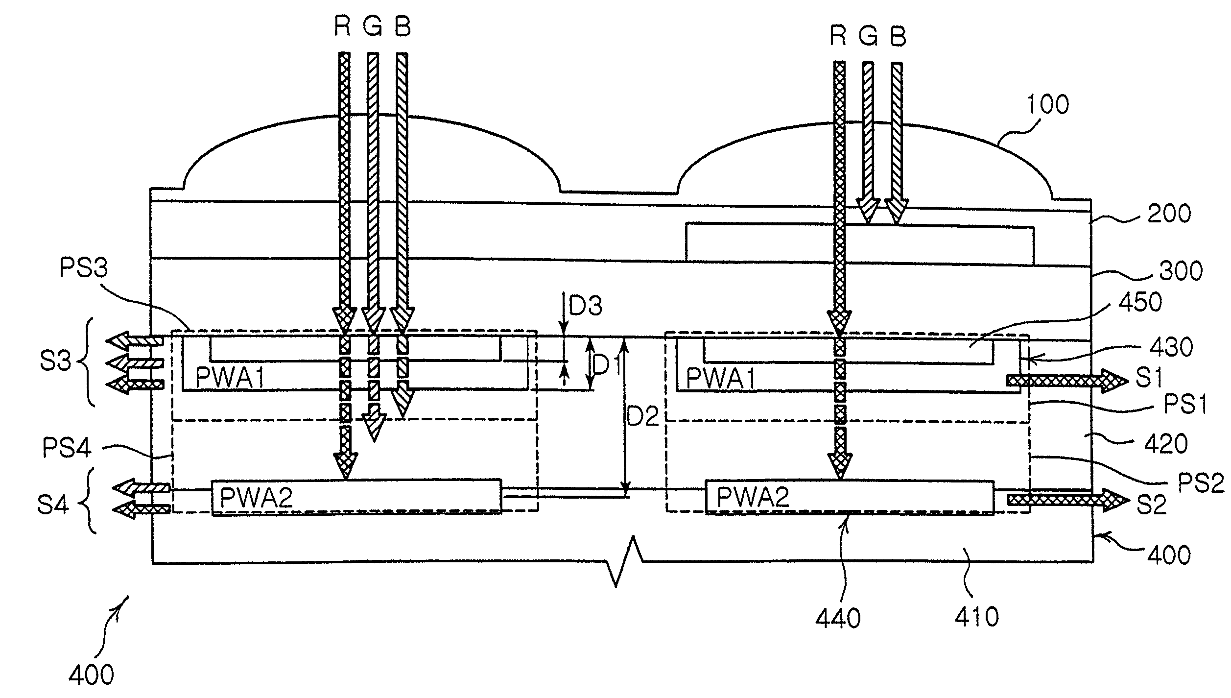
[0055]With reference to FIG. 5, the image processing apparatus according to the present invention includes an image sensor (IMS) for sensing light from an object image and a signal processor 500 for processing a signal from the IMS.

[0056]With reference to FIG. 5, the IMS includes a lens array 100, a color filter array 200, a protection layer 300 and a pixel sensor array 400 each formed in a silicon semiconductor. The lens array 100 includes a plurality of microlenses 110 formed in a two-dimensional matrix. Here, each microlens focuses the incident light to a predetermined region.

[0057]FIG. 6 is a diagram illustrating a pattern of a ...


PUM


Abstract

An image sensor for an image processing apparatus having a color filter array with open window cells alternating with single color filter cells includes a lens array containing a plurality of microlenses, a color filter array having a plurality of open window cells and color filter cells, each corresponding to one microlens. The image sensor also includes a protection layer, and a pixel sensor array having a first photosensor sensing a first light passed through each color filter cell, a second photosensor formed under the first photosensor, sensing a second light passed through each color filter cell, a third photosensor sensing a third light passed through each open window cell, and a fourth photosensor formed under the third photosensor, sensing a fourth light passed through each open window cell.

Description

CLAIM OF PRIORITY[0001]This application claims the benefit of Korean Patent Application No. 2005-44149 filed on May 25, 2005, in the Korean Intellectual Property Office, the disclosure of which is incorporated herein by reference.BACKGROUND OF THE INVENTION[0002]1. Field of the Invention[0003]The present invention relates to an image sensor and an image processing apparatus adopted in camcorders, digital cameras, etc. More particularly, the invention relates to an image sensor for semiconductor light-sensing device which uses a color filter array having open windows and single-color filters alternating with each other, using information of a plurality of colors for each pixel to allow more accurate interpolation, thereby extracting a more accurate color for each pixel, and to an image processing apparatus using the same.[0004]2. Description of the Related Art[0005]In general, the recent developments in the picture communication by wire / wireless high-speed network system, and the pic...

Claims


Application Information

Patent Timeline
Patent Type & Authority Patents(United States)
IPC IPC(8): G01J3/50H01J40/14H01J5/16H01L27/14H01L27/146H04N9/07
CPCH01L27/14621H01L27/14627H01L27/14647H04N9/045H01L31/02162H04N2209/047H04N25/134H01L27/146
Inventor KANG, SHIN JAECHOI, WON TAEKO, JOO YULPARK, DEUK HEE
Owner SAMSUNG ELECTRO MECHANICS CO LTD
Why Eureka
Try Eureka