Method of manufacturing liquid crystal display device

A technology of a liquid crystal display device and a manufacturing method, which are applied in the photoengraving process of the pattern surface, the exposure device of the photoengraving process, optics, etc., can solve the problems such as the inability to properly correct the positional deviation and the like

Inactive Publication Date: 2007-01-31
MITSUBISHI ELECTRIC CORP
View PDF3 Cites 11 Cited by
  • Summary
  • Abstract
  • Description
  • Claims
  • Application Information

AI Technical Summary

Problems solved by technology

[0011] When manufacturing a large liquid crystal display device, there are cases where the display area is larger than the irradiation area, but in this case, Patent Documents 1 to 3 have a problem that positional deviation cannot be properly corrected

Method used


Image

  • Method of manufacturing liquid crystal display device
  • Method of manufacturing liquid crystal display device
  • Method of manufacturing liquid crystal display device

Examples


Embodiment 1

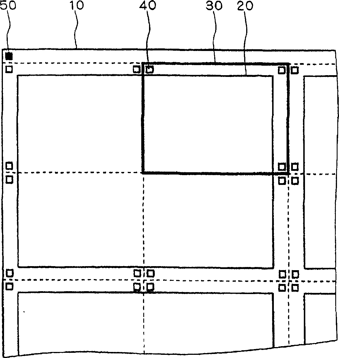
[0029] figure 1 It is a plan view showing an example of an array substrate used in the liquid crystal display device of Example 1.

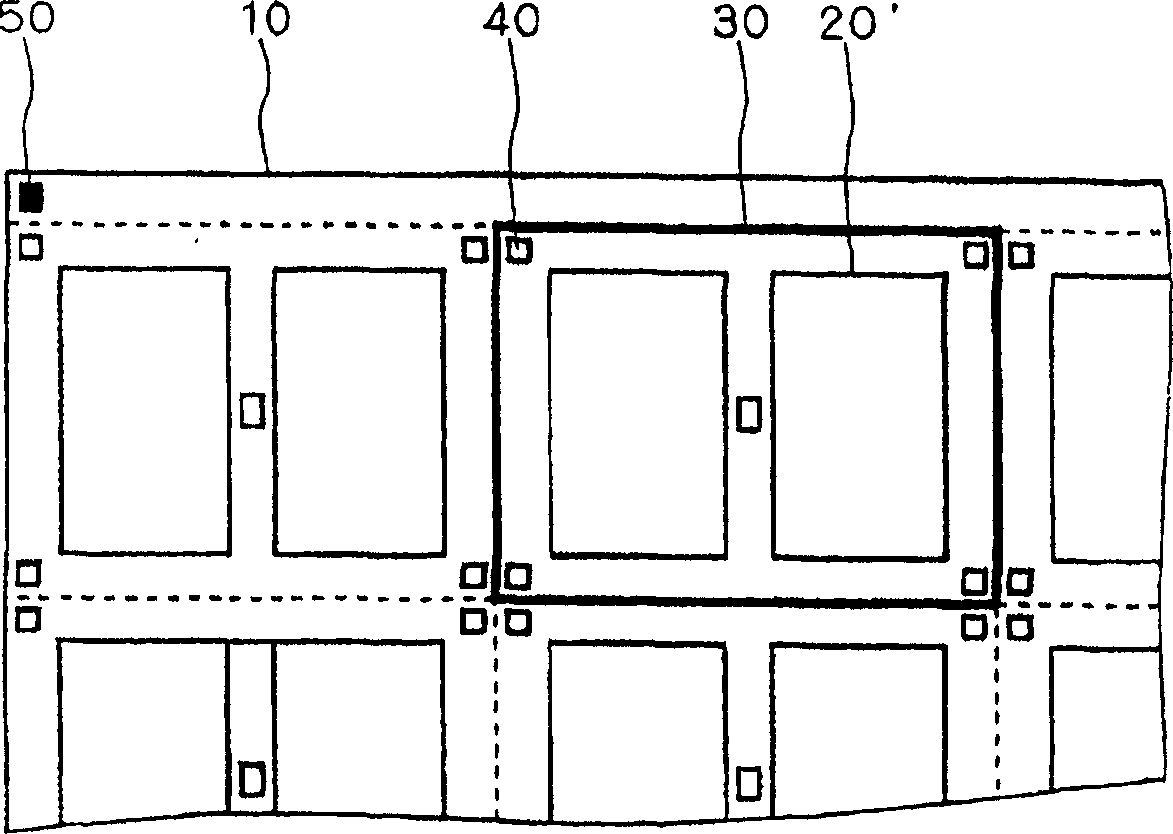
[0030] Such as figure 1 As shown, on the array substrate 10, a plurality of display regions 20 corresponding to one display substrate mounted on one liquid crystal display device are formed in parallel by stepper exposure. On the display area 20 are formed pixel electrodes, thin film transistors, source wiring, gate wiring, etc. ( figure 1 not shown). The array substrate 10 is divided into array shot regions 30 (thick line portions) serving as irradiation units in the divided exposure. figure 1 One display area 20 is divided into four array irradiation areas 30 . That is, one array irradiation area 30 includes 1 / 4 display area 20 .

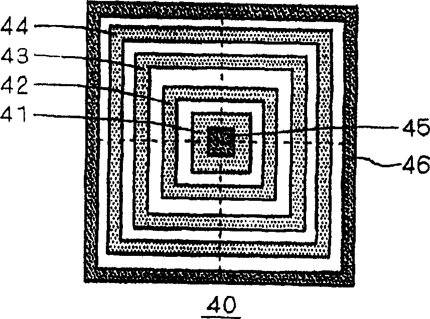
[0031] At least one positioning mark 40 is provided in one array irradiation area 30 ( figure 1 3 of them). In addition, the array substrate 10 has a rectangular shape, and superimposing marks 50 serving as a ...


PUM


Abstract

A plurality of display areas are formed on an array substrate by stepper exposure. The array substrate is divided into array shot areas serving as shot units at the time of divided exposure. One display area is divided into four array shot areas. One array shot area is provided with at least one alignment mark. The array substrate has a rectangular shape, and is provided with a superimposition mark at the corner thereof which is used as the reference for superimposing the array substrate and a CF substrate.

Description

technical field [0001] The invention relates to a manufacturing method of a liquid crystal display device, in particular to a technology for improving the overlapping accuracy of an array substrate and a color filter substrate. Background technique [0002] With the recent improvement of high precision and display quality of liquid crystal display devices, the requirements for the overlapping accuracy of the array substrate and the color filter substrate are becoming more and more stringent. [0003] In order to improve the overlay accuracy, it is obvious that it is extremely important to eliminate deviations during superimposition, and to form each pattern on the array substrate and the color filter substrate with high precision without deviation. [0004] If the area corresponding to one display substrate mounted on one liquid crystal display device is called the display area, the array substrate and the color filter substrate are both formed on a large glass substrate, an...

Claims


Application Information

Patent Timeline
Patent Type & Authority Applications(China)
IPC IPC(8): G02F1/1333G03F7/20
CPCG03F7/70791G03F7/70425G03F9/7084G02F1/1333
Inventor 藤田康雄
Owner MITSUBISHI ELECTRIC CORP
Why Eureka
Try Eureka