Semiconductor device

A technology for semiconductors and devices, applied in the field of semiconductor devices, can solve the problem of inability to obtain the resistance ratio, and achieve the effects of accurate resistance ratio, stable resistance ratio, and preventing the increase of manufacturing cost.

Active Publication Date: 2015-06-10
SII SEMICONDUCTOR CORP
View PDF4 Cites 0 Cited by
  • Summary
  • Abstract
  • Description
  • Claims
  • Application Information

AI Technical Summary

Problems solved by technology

However, in many cases, the desired resistance ratio cannot be obtained, and a resistance ratio of, for example, 1:1.7 is obtained

Method used


Image

  • Semiconductor device
  • Semiconductor device
  • Semiconductor device

Examples


Embodiment

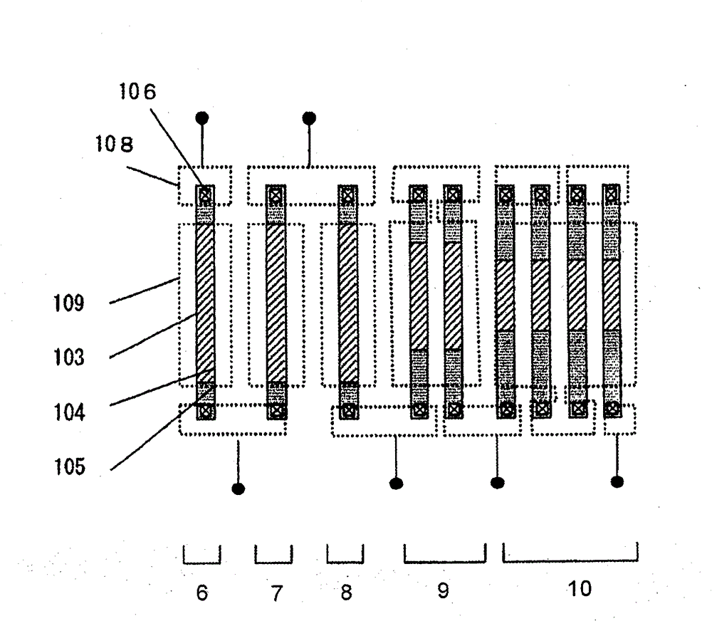
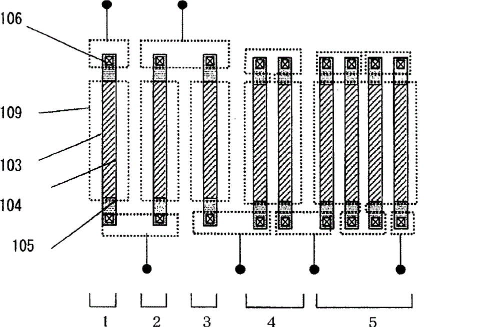
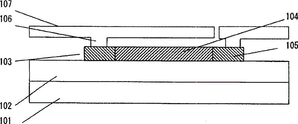
[0026] image 3 Showing a 50 µm increase in the area of ​​the second metal part 2 Increased the resistance ratio by 1%. This establishes the expression described below.

[0027]Assuming that the resistance ratio desired to be increased is a%, the area of ​​the second metal portion is A, the area of ​​the low-concentration impurity region before changing the area is B, and the area of ​​the low-concentration impurity region changed to change the resistance ratio is X1. To increase the resistance ratio by a%, multiply 50 by a and add to A. However, the area of ​​the second metal portion is not changed in the present invention. Therefore, the equation (A+50·a):B=A:X1 holds true, and X1 is expressed by the equation X1=A·B / (A+50·a). Further, in the present invention, the length L of the low-concentration impurity region in the longitudinal direction is changed, thereby changing the area. When the area of ​​the low-concentration impurity region is expressed as the equation X1=(...


PUM


Abstract

Provided is a method capable of forming a polycrystalline silicon resistor with preferable ratio accuracy so as to design a resistor circuit with high accuracy. In the method, a length of a low concentration impurity region constituting the polycrystalline silicon resistor in a longitudinal direction is varied in accordance with an occupying area of a metal portion overlapping the low concentration impurity region, thereby correcting a variation in resistance without varying an external shape and the occupying area of the resistor.

Description

technical field [0001] The present invention relates to a semiconductor device comprising a resistor made of polysilicon. Background technique [0002] In semiconductor integrated circuits, diffused resistors or polysilicon resistors are used. The diffused resistor is made of a single crystal silicon semiconductor substrate into which impurities of a conductivity type opposite to that of the semiconductor substrate are implanted. Polysilicon resistors are made of polysilicon into which impurities have been implanted. In particular, polysilicon resistors have advantages such as small leakage current caused by an insulating film surrounding the resistor and high resistivity due to defects present at grain boundaries, making them widely used in semiconductor integrated circuits. [0003] Figure 2A and 2B Respectively, a schematic plan view and a schematic cross-sectional view of a conventional polysilicon resistor circuit. Polysilicon resistors are formed by injecting p-ty...

Claims


Application Information

Patent Timeline
Patent Type & Authority Patents(China)
IPC IPC(8): H01L27/04
CPCH01L28/20
Inventor 塚本明子原田博文
Owner SII SEMICONDUCTOR CORP
Why Eureka
Try Eureka