MEMS probe card and manufacturing method thereof

Pending Publication Date: 2011-04-21
TOP ENG CO LTD
View PDF11 Cites 17 Cited by
  • Summary
  • Abstract
  • Description
  • Claims
  • Application Information

AI Technical Summary

Benefits of technology

The present invention is directed to a MEMS probe card, which can obtain a stable resistance ratio at a high temper

Problems solved by technology

However, the necessity for downsizing the probe card complicates the manufacture of the probe card.
However, even when only one channel is short-circuited in the multichannel probe, an excessive current flows through the corresponding channel, which may cause a spark-induced failure at probe terminals.
However, since the thin film resistor 12 is connected to the thin film conductive line 13 of the conventional MEMS probe card in series in an X or Y direction, the circuit integration is lowered, and this problem becomes more serious when the thin film resistor 12 is designed in the form of a bar.
However, since the tungsten conductive line fired at a high te

Method used


Image

  • MEMS probe card and manufacturing method thereof
  • MEMS probe card and manufacturing method thereof
  • MEMS probe card and manufacturing method thereof

Examples


first exemplary embodiment

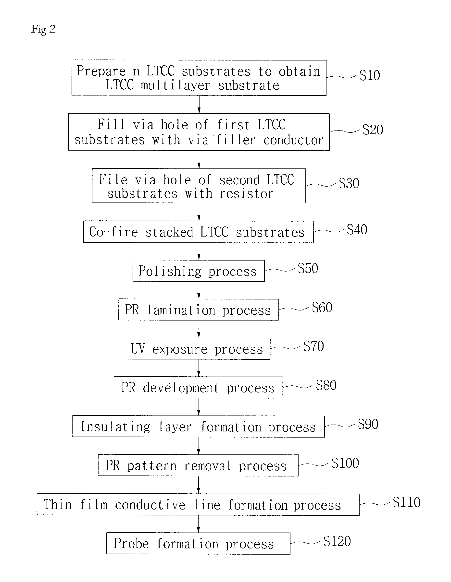
FIG. 2 is a diagram illustrating a method for manufacturing a MEMS probe card in accordance with a first exemplary embodiment of the present invention, and FIGS. 3 to 10 are diagrams illustrating the individual processes shown in FIG. 2.

As shown in FIGS. 2 and 3, in this exemplary embodiment of the present invention, n LTCC substrates are prepared to obtain an LTCC multilayer substrate 100 (S10). The number of layers of the LTCC multilayer substrate 100 may vary according to the substrate design and is preferably 20 to 30 layers according to the test conditions of semiconductor chips. Here, silver (Ag) is mainly used as a material for a metal wiring, and the composition may vary, if necessary. Moreover, ceramic materials used in the LTCC substrate include more than 60 to 70% glass and the remaining alumina. The thickness of each LTCC substrate may vary according to requirements of customers, and is preferably 4 to 7 mm.

Meanwhile, a via hole 1 penetrates each LTCC substrate, and a co...

second exemplary embodiment

FIG. 11 is a diagram illustrating a method for manufacturing a MEMS probe card in accordance with a second exemplary embodiment of the present invention, and FIGS. 12 to 21 are diagrams illustrating the individual processes shown in FIG. 11.

As shown in FIG. 12, in this exemplary embodiment, an LTCC multilayer substrate 100 including n LTCC substrates are prepared (S10). The number of layers of the LTCC multilayer substrate may vary according to the substrate design and is preferably 20 to 30 layers. Here, silver (Ag) is mainly used as a material for a metal wiring, and the composition may vary, if necessary. Ceramic materials used in the LTCC substrate include more than 60 to 70% glass and the remaining alumina. The thickness of each LTCC substrate may vary according to requirements of customers, and is preferably 4 to 7 mm. In FIG. 12, reference numeral 1 denotes a via hole (through hole) formed in the substrate, and reference numeral 2 denotes a conductive line formed in the subst...


PUM

PropertyMeasurementUnit
Temperatureaaaaaaaaaa
Thicknessaaaaaaaaaa
Dielectric polarization enthalpyaaaaaaaaaa

Abstract

Provided are a micro-electro-mechanical system (MEMS) probe card and a method for manufacturing the same. The method includes preparing first to nth low-temperature co-fired ceramic (LTCC) substrates each having a via hole, filling each via hole with a via filler conductor or a resistor, stacking the first to nth LTCC substrates and firing the stacked substrates at a temperature of 1,000° C. or less to prepare a LTCC multilayer substrate, forming an insulating layer on the surface of the LTCC multilayer substrate, and forming a thin film conductive line on the surfaces of the insulating layer and the via filler conductor.

Description

BACKGROUND OF THE INVENTION1. Field of the InventionThe present invention relates to a micro-electro-mechanical system (MEMS) probe card and a method for manufacturing the same, and more particularly, to a MEMS probe card and a method for manufacturing the same, in which a resistive conductive line is formed on a low-temperature co-fired ceramic (LTCC) multilayer substrate such that a stable resistance ratio can be obtained and the MEMS probe card can be stably used in the event of a significant change in power, and a ruthenium oxide (e.g., Ru2O3) having stable characteristics with respect to the surface of the substrate is used as the resistive conductive line so as to facilitate design of electric power distribution.2. Description of Related ArtIn general, a probe card used in a test device for electronic components such as semiconductor chips is a device including a predetermined substrate and probes arranged on the substrate. The probe card is used to test electrical characteris...

Claims


Application Information

Patent Timeline
IPC IPC(8): G01R31/00C03B29/04H01B13/16H01L21/302
CPCB81B2203/0118B81C99/005G01R3/00H01L2924/0002H01L2924/00
Inventor KIM, SANGHEE
Owner TOP ENG CO LTD
Why Eureka
Try Eureka