MEMS probe card and method of manufacturing same

a micro-electromechanical system and probe card technology, applied in the field of micro-electromechanical system (mems) probe cards, can solve the problems of difficult application of thin film resistors, complicated manufacture of probe cards, and spark-induced failure of probe terminals, etc., to achieve stable resistance ratio, easy control of resistance value, and use stably

Inactive Publication Date: 2011-07-14
TOP ENG CO LTD
View PDF9 Cites 10 Cited by
  • Summary
  • Abstract
  • Description
  • Claims
  • Application Information

AI Technical Summary

Benefits of technology

[0025]The present invention is also directed to a MEMS probe card and a method for manufacturing there of, in which the stability of contact pattern between resistive film and electrode can be kept by making the contact area big.
[0026]The present invention is also directed to a MEMS probe card and a method for manufacturing thereof, in which the stable resistance ratio can be obtained within the space at a narrow substrate from forming the second conductive line after coating the insulation layer, and the probe card can be stably used in the event of a significant change in power.
[0027]The present invention is also directed to a MEMS probe card and a method for manufacturing thereof, in which the ratio of resistance value can be easily controlled.
[0028]The present invention is also directed to a MEMS probe card and a method for manufacturing thereof, in which the pattern of thin film resistor and thin film conductive line is accurate and precise resistance value can be obtained.

Problems solved by technology

However, the necessity for downsizing the probe card complicates the manufacture of the probe card.
However, even when only one channel is short-circuited in the multichannel probe, an excessive current flows through the corresponding channel, which may cause a spark-induced failure at probe terminals.
In the conventional thin film resistor substrate, however, it is difficult to apply the thin film resistor 12 to the MEMS probe card which requires high electric power by the increase of I / O pins of semiconductor IC when the thin film resistor 12 is designed to have a width equal to or smaller than that of the electrode 13.
In the structure as shown in FIG. 1, there has also been the problem that the pattern stability becomes lowered due to the small contact area between the resistive film 12 and the electrode 13.
In addition, in the conventional thin film resistor substrate, there is the problem that it is difficult to form a plurality of resistive film 12 against the increase of I / O pins of semiconductor IC and the probe tip; that is, the problem that it is difficult to form a plurality of resistive film having the desirable resistance value within the predetermined space.
Furthermore, since the thin film resistor 12 is connected to the thin film conductive line 13 of the conventional MEMS probe card in series in an X or Y direction, the circuit integration is lowered, and this problem becomes more serious when the thin film resistor 12 is designed in the form of a bar.
However, since the tungsten conductor fired at a high temperature has an electrical conductivity lower than that of silver (Ag) or copper (Cu), it has inferior high frequency characteristics.
Moreover, since the thermal expansion coefficient of the tungsten conductive line is more than two times as high as a silicon semiconductor device, it is a serious problem in the field of application where matching of thermal expansion coefficients is required.
However, despite the above advantages, the LTCC multilayer substrate has a rough surface, and thus it is difficult to form a thin film resistor having a thickness of several tens to several hundreds of nanometers (nm) on the surface of the LTCC multilayer substrate.

Method used


Image

  • MEMS probe card and method of manufacturing same
  • MEMS probe card and method of manufacturing same
  • MEMS probe card and method of manufacturing same

Examples


first exemplary embodiment

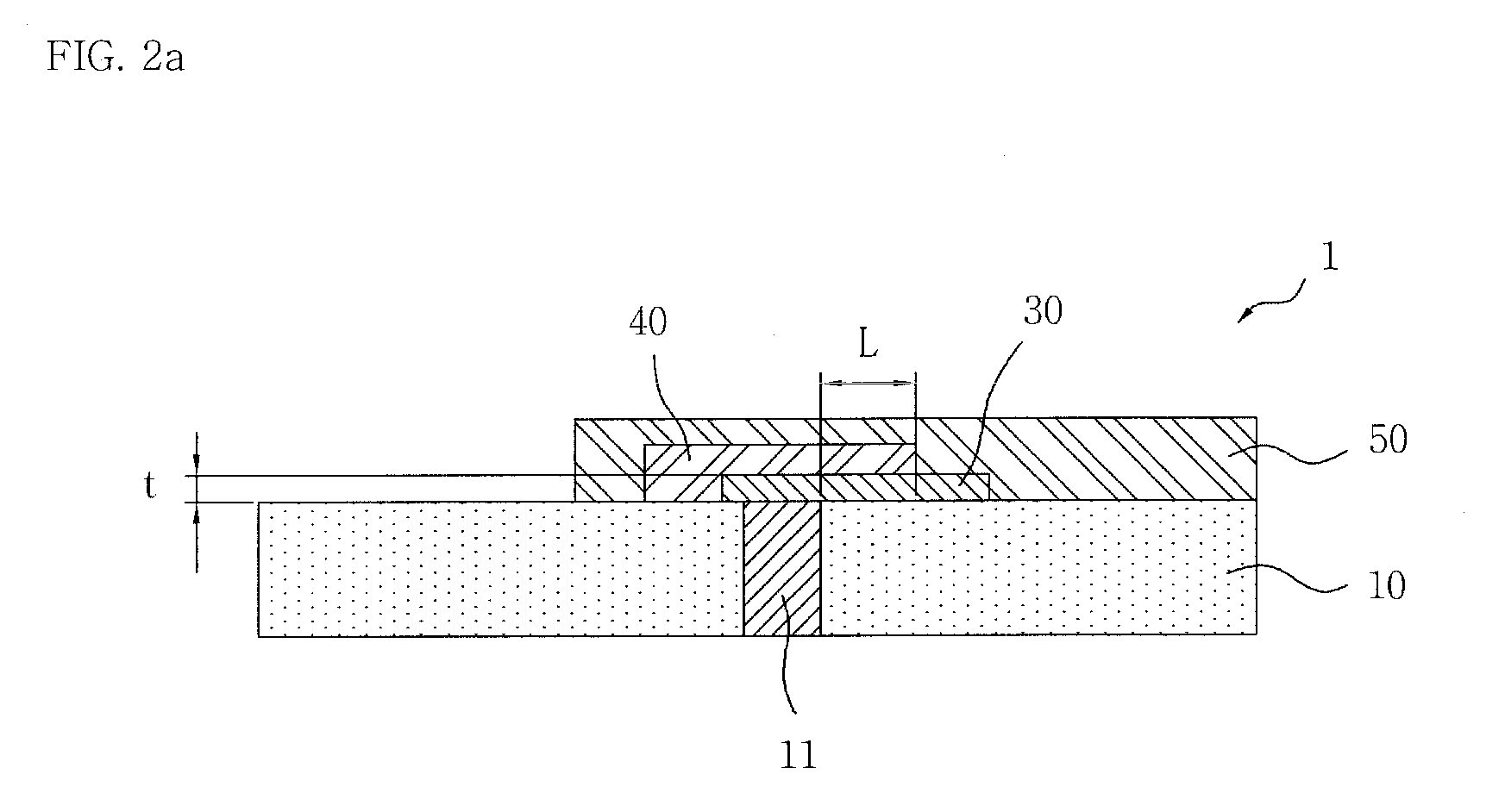
[0091]FIG. 2a and 2b are a cross sectional view of a thin film resistor substrate and illustration of the pattern in accordance with a first exemplary embodiment of the present invention.

[0092]First, the concept of a thin film resistor substrate by using an insulating film in accordance with a first exemplary embodiment of the present invention, will be described.

[0093]In the thin film resistor substrate, the decisive variables of resistance value(R) are k, the specific resistance value of a resistive film; t, the thickness of a resistive film and L, the length of a resistive film (the length of the duplicated part of the resistive film and an insulating film excluding the via hole, in FIG. 2); and d, the width of the resistive film.

[0094]Accordingly, the resistance value, as the following formula, is in proportion to the specific resistance value and length of material, and in inverse proportion to thickness and width.

R∝k(L / A)   

[0095]The passage area of resistance, A=t*d.

[0096]As ...

second exemplary embodiment

[0130]First, the formula 1 of the first exemplary embodiment is still applied to the second exemplary embodiment of the present invention.

[0131]As shown in FIG. 6 to 8, in the exemplary embodiment of the present invention, a substrate 1 having a via hole 2 filled with a via hole filler conductor or resistor is prepared, and then the thin film resistive line 3 is formed on the via hole 2 and the substrate 1(S10).

[0132]The via filler conductor 4 may be formed of a metal selected from silver (Ag), palladium (Pd), and platinum (Pt), and preferably Pd or Pt in view of conductivity. The use of TaN is preferable for the material of the thin film resistive line 3.

[0133]To describe the forming method of the thin film resistive line 3, as shown in FIG. 7, TaN is coated on the whole surface of the substrate 1 in a sputtering manner. Then, a process of laminating dry photoresist (PR) thickly on the surface of the substrate using a laminator is performed. Here, the pressure, temperature, and spe...

third exemplary embodiment

[0151]First, the formula 1 of the first exemplary embodiment is still applied to the third exemplary embodiment of the present invention as the third exemplary embodiment is for the LTCC multilayer having the thin film resistor.

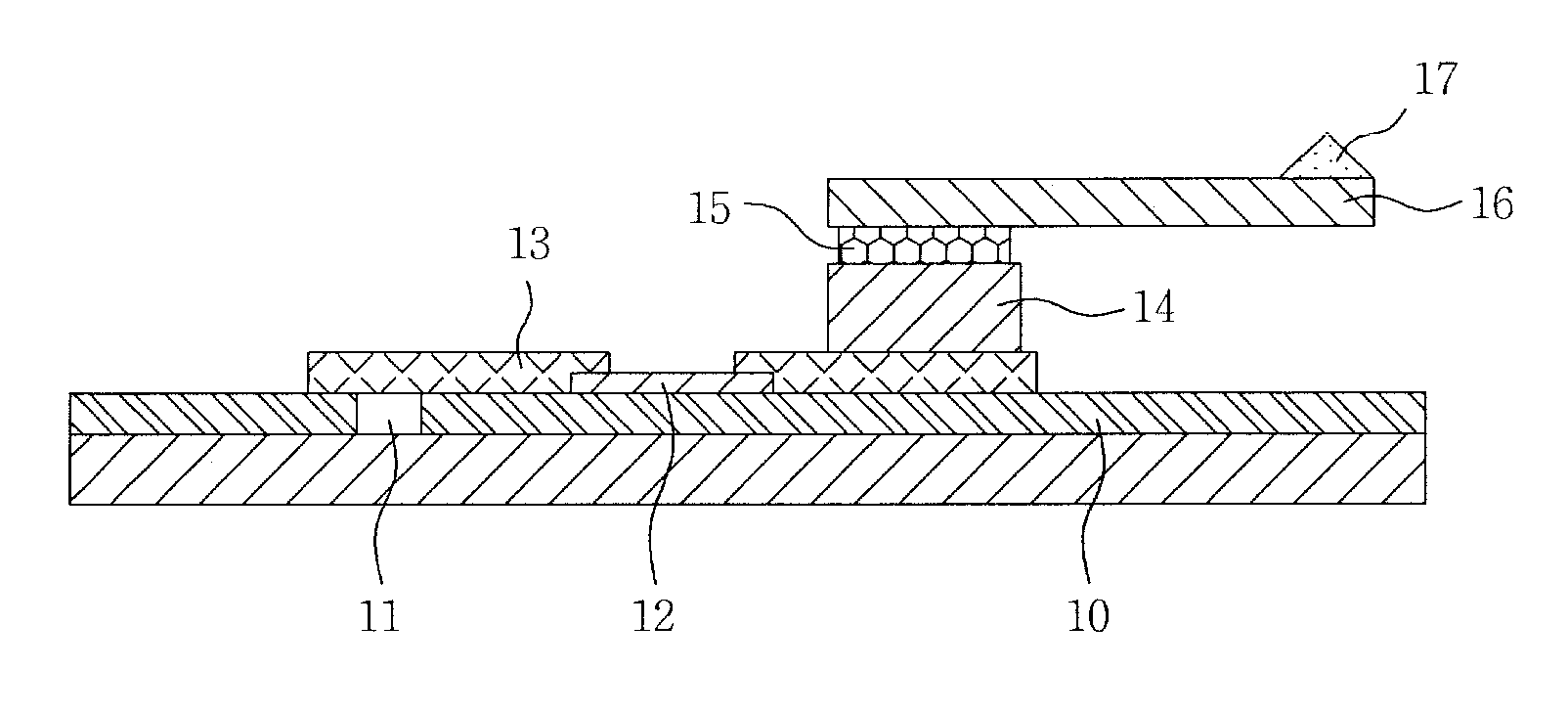
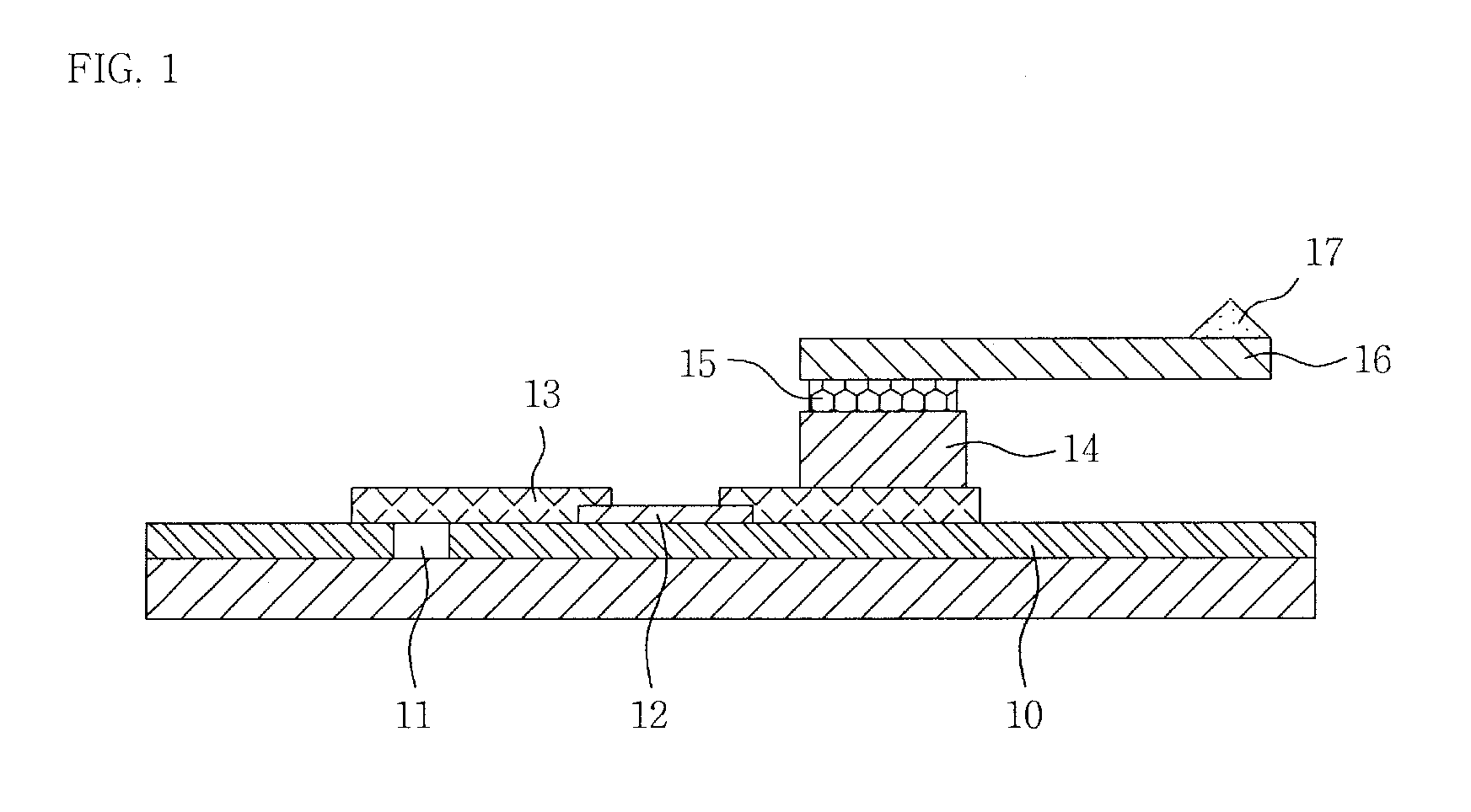
[0152]FIG. 16 is a cross sectional view of the MEMS probe card in accordance with the present invention.

[0153]As shown in FIG. 16, the micro-electro-mechanical system (MEMS) probe card in the present invention includes; a low-temperature co-fired ceramic (LTCC) multilayer substrate(100) prepared by stacking first to nth LTCC substrates; the upper conductive line 6 prepared on the LTCC multilayer substrate(100) and formed with via hole filled with via hole filler conductor 4; the thin film resistor 7 formed on the upper conductive line 6; the first thin film conductive line 8 formed on the upper conductive line 6; the thin film resistor 7 and via hole filler conductor 4; the insulating film 9 formed on the thin film resistor 7 and the first thin film conductiv...


PUM


Abstract

Provided are a micro-electro-mechanical system (MEMS) probe card and a method for manufacturing thereof. The MEMS probe card includes a substrate provide with a via hole filler conductor or a via hole filled with the resistor, the resistive film formed on the via hole and the substrate, the insulating film and the resistive film formed on the resistive film and the substrate, and the electrode formed on the substrate to cover the insulating film
As such, by means of a micro-electro-mechanical system (MEMS) probe card and a method for manufacturing thereof, the precise resistance value can be obtained and used for the semiconductor IC and others in the event of significant change in power.

Description

BACKGROUND OF THE INVENTION[0001]1. Field of the Invention[0002]The present invention relates to a micro-electro-mechanical system (MEMS) probe card of high chemical resistance and a method for manufacturing thereof, and more particularly, to a MEMS probe card and a method for manufacturing thereof, in which a stable resistance ratio can be obtained, and the MEMS probe card can be used in the event of significant change in power, and a precise resistive conductive line can be formed[0003]2. Description of Related Art[0004]In general, a probe card used in a test device for semiconductor IC and such is a device including a predetermined substrate and probes arranged on the substrate. The probe card is used to test electrical characteristics of micro electronic device such as semiconductor device.[0005]The semiconductor device includes pads on its surface to transmit and receive signals to and from an external electronic device. That is, the semiconductor device receives an electrical ...

Claims


Application Information

Patent Timeline
Patent Type & Authority Applications(United States)
IPC IPC(8): G01R31/00
CPCG01R1/06744G01R1/06727G01R3/00
Inventor KIM, SANG-HEELEE, SANG HYUNLEE, JAE SEOKWOO, CHUN SIKLEE, JAE IN
Owner TOP ENG CO LTD
Why Eureka
Try Eureka