Optoelectronic component, device comprising a plurality of optoelectronic components, and method for the production of an optoelectronic component

A technology for optoelectronic components and active areas, applied in electrical components, electrical solid state devices, circuits, etc., can solve problems such as difficulty in constructing small optoelectronic components, and achieve the effect of avoiding single processing steps and reducing the risk of short circuits

Inactive Publication Date: 2007-02-28
OSRAM OPTO SEMICONDUCTORS GMBH & CO OHG
View PDF2 Cites 14 Cited by
  • Summary
  • Abstract
  • Description
  • Claims
  • Application Information

AI Technical Summary

Problems solved by technology

The housing, which is constructed separately from the semiconductor functional area, often has significantly larger spatial dimensions than the semiconductor functional area, which can also make the construction of small optoelectronic components difficult

Method used


Image

  • Optoelectronic component, device comprising a plurality of optoelectronic components, and method for the production of an optoelectronic component
  • Optoelectronic component, device comprising a plurality of optoelectronic components, and method for the production of an optoelectronic component
  • Optoelectronic component, device comprising a plurality of optoelectronic components, and method for the production of an optoelectronic component

Examples


Embodiment Construction

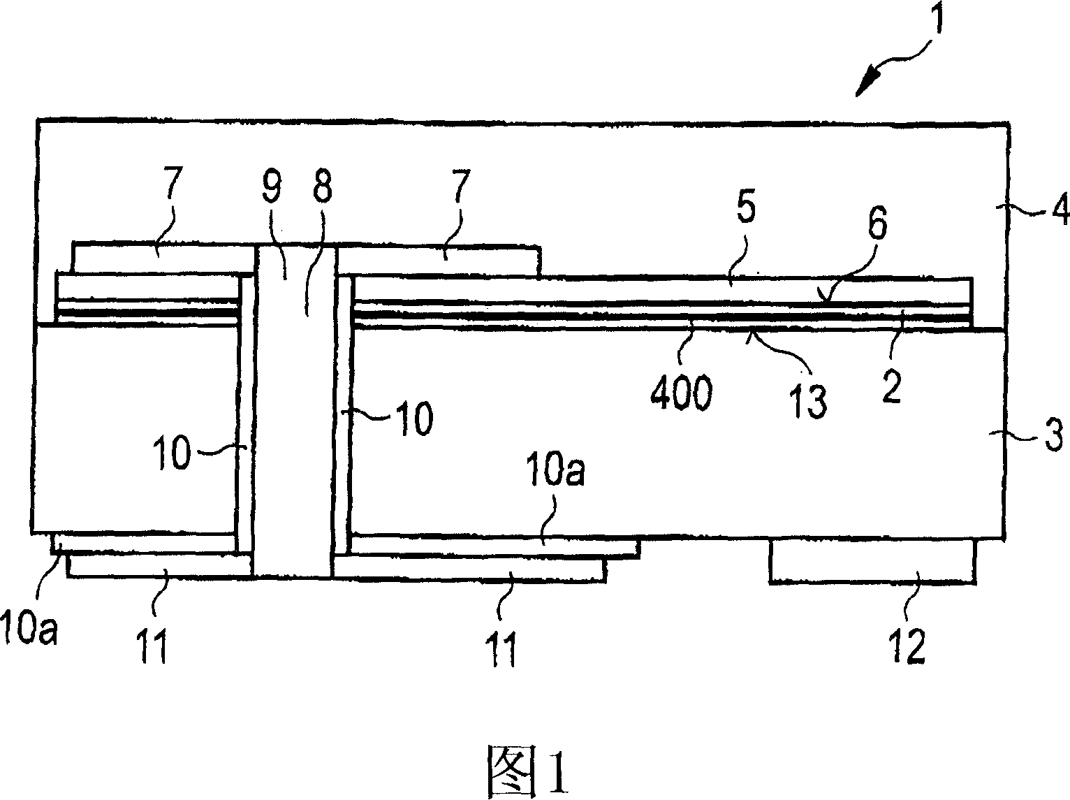
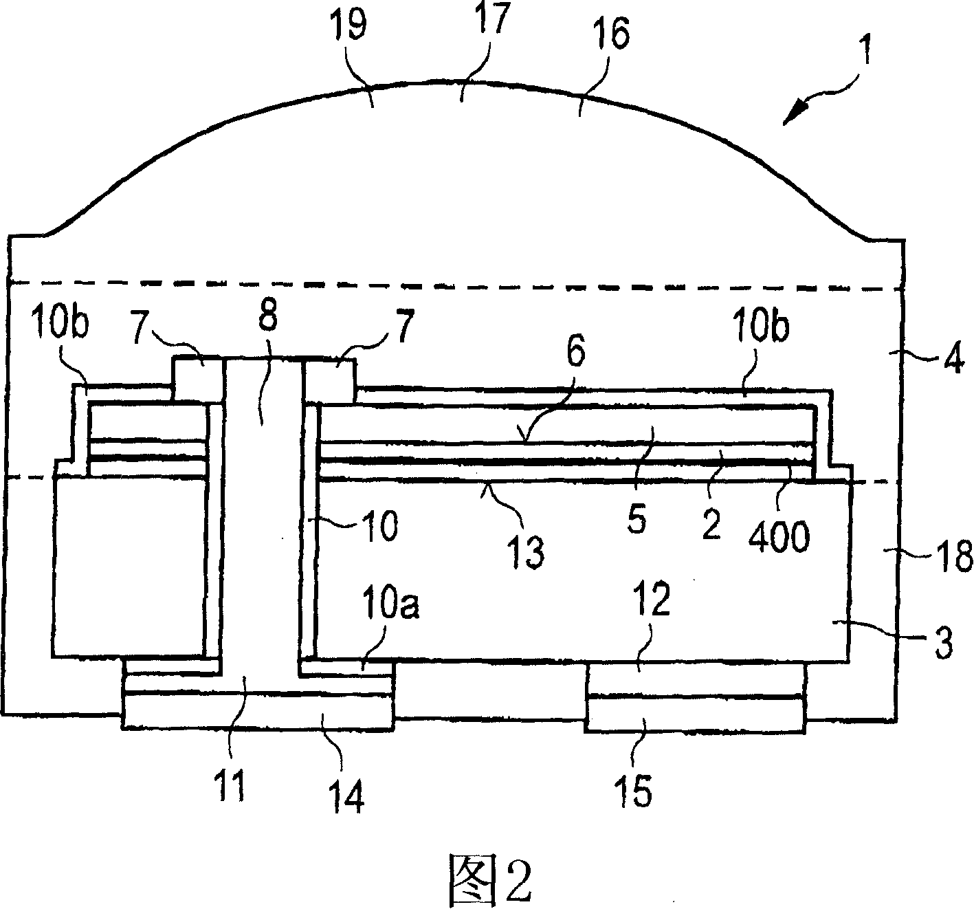
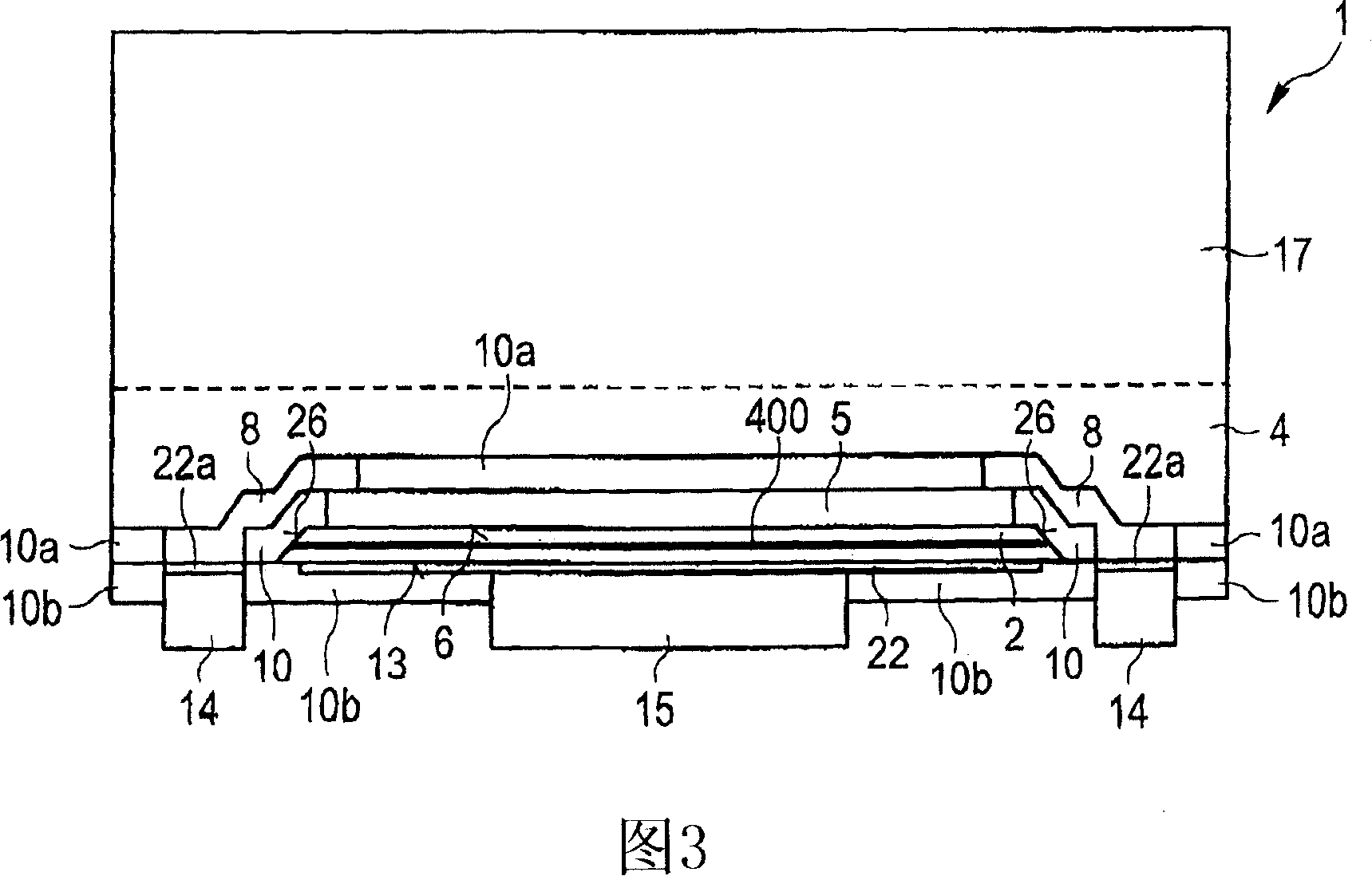
[0156] Elements of the same type and function are provided with the same reference numerals in the figures.

[0157] A first exemplary embodiment of an optoelectronic component according to the invention is shown in FIG. 1 with the aid of a schematic sectional illustration.

[0158] The optoelectronic component 1 comprises a semiconductor functional region 2 arranged on a carrier 3 . The semiconductor functional region comprises an active region 400 provided for radiation generation or radiation reception and has a transverse main direction of extension.

[0159] The active region may, for example, comprise a heterostructure, in particular a double heterostructure, a single or multiple quantum well structure or a pn junction.

[0160] The semiconductor functional region 2 , in particular its active region 400 , for example comprises a plurality of semiconductor layers and / or is for example based on GaN or GaP. If the semiconductor functional region is based on GaP, the optoe...


PUM


Abstract

The component has a functional semiconductor area (2) with an active zone (400) and a lateral principal direction of extension. The area is provided with a breakthrough in the active zone. A connecting conductor material (8) is electrically isolated from the active zone in a subarea of the breakthrough and is arranged in a region of the breakthrough. The breakthrough is partially covered by an insulating material (10). - Independent claims are also included for the following: - (A) a device with optoelectronic components - (B) a method for manufacturing an optoelectronic component.

Description

technical field [0001] The invention relates to an optoelectronic component according to the preamble of claim 1 , a device according to the preamble of claim 16 and a method according to the preamble of claim 21 . Background technique [0002] In the manufacture of conventional optoelectronic components of this type, single processing steps are generally required, such as, for example, arranging the semiconductor functional area or a semiconductor chip comprising the semiconductor functional area in a housing, contacting the semiconductor chip with external terminals by bonding wires, or Protective encapsulation (Umhuellung) for the injection molding of semiconductor chips. Single processing steps are often cost intensive compared to processing steps that can be performed on multiple elements simultaneously. [0003] The semiconductor functional region can be formed, for example, from a semiconductor layer sequence in a wafer bond, wherein the wafer bond includes the semic...

Claims


Application Information

Patent Timeline
Patent Type & Authority Applications(China)
IPC IPC(8): H01L27/15H01L27/14H01L31/0224H01L33/00H01L33/38
CPCH01L33/382H01L33/0079H01L31/022416H01L33/0095H01L31/022408H01L2224/16225H01L33/0093H01L31/02
Inventor 拉尔夫·维尔特赫贝特·布伦纳斯特凡·伊莱克迪特尔·艾斯勒
Owner OSRAM OPTO SEMICONDUCTORS GMBH & CO OHG
Why Eureka
Try Eureka