Image display device and driving method thereof

A technology of image display and driving method, applied in static indicators, instruments, etc., can solve problems such as difficulty in improving fineness, and achieve the effects of improving fineness, reducing resistance, and improving contrast.

Active Publication Date: 2007-05-02
LG DISPLAY CO LTD
View PDF0 Cites 4 Cited by
  • Summary
  • Abstract
  • Description
  • Claims
  • Application Information

AI Technical Summary

Problems solved by technology

In this way, the image display device of the prior art is still a 3TFT structure or a 4TFT structure in the practical stage, and there is a problem that it is difficult to improve the fineness.

Method used


Image

  • Image display device and driving method thereof
  • Image display device and driving method thereof
  • Image display device and driving method thereof

Examples


Embodiment Construction

[0038]

Embodiments of the image display device according to the present invention will be described in detail below with reference to the drawings. In addition, the present invention is not limited to employing this embodiment mode.

[0039]

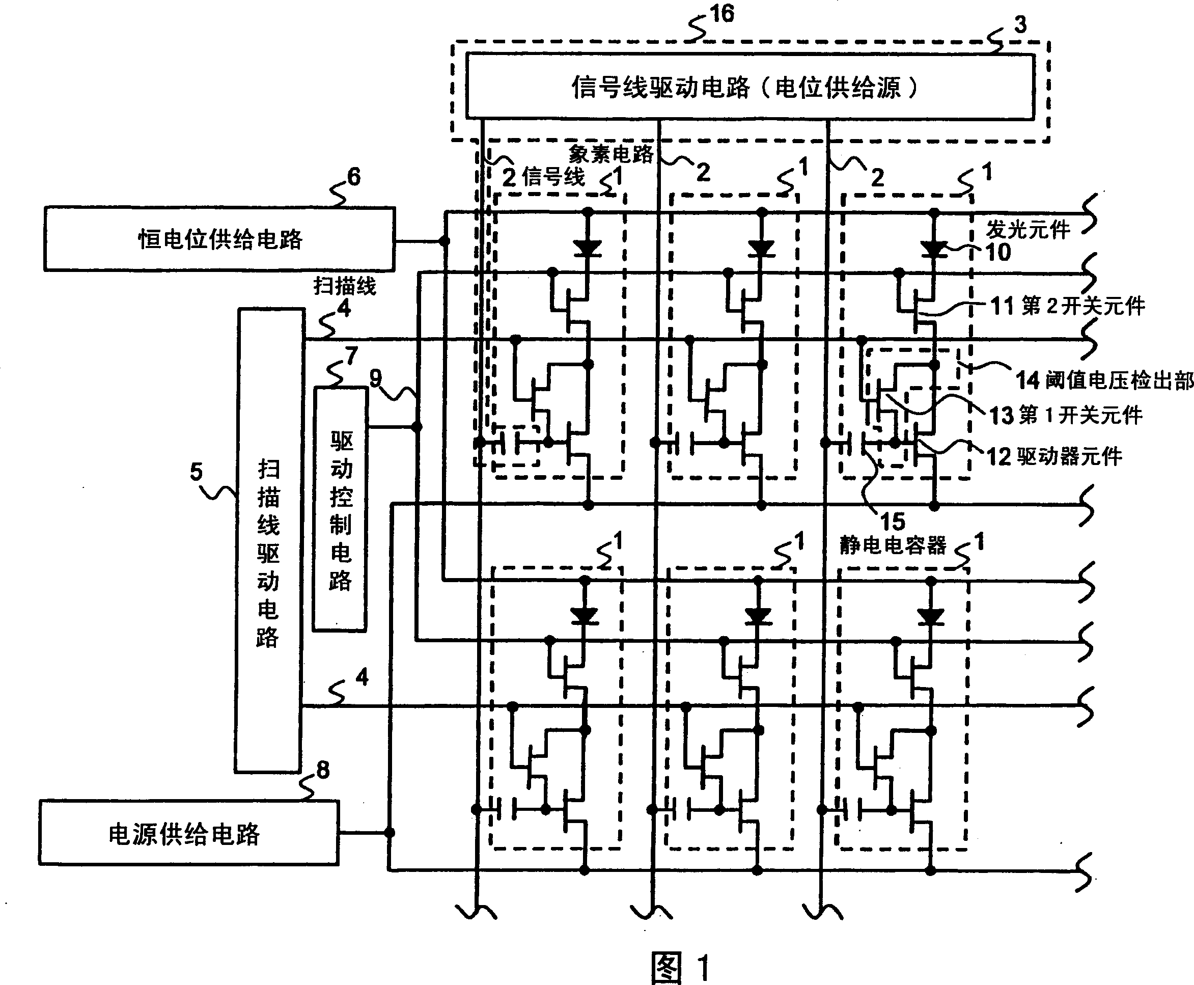
FIG. 1 is a diagram showing the overall configuration of an image display device according to a first embodiment of the present invention. The image display device shown in FIG. 1 has a function of preventing light emission in a reset step that should improve contrast, and has a plurality of pixel circuits 1 (these pixel circuits 1 are arranged in rows and columns), a signal line driver circuit 3 (the The signal line driver circuit 3 supplies a plurality of pixel circuits 1 with luminance signals described later through the intermediary of the plurality of signal lines 2), and the scanning line driver circuit 5 (the scanning line driver circuit 5 uses the plurality of scanning lines 4 as the intermediary). , to supply the pixel circui...


PUM


Abstract

An image display device is provided with a light emitting element; a driving transistor wherein a gate electrode, a source electrode and a drain electrode are provided and one edge of the light emitting element is electrically connected with one of the electrodes of the source electrode and the drain electrode; a first switching transistor, which short-circuits the gate electrode of the driving transistor and the one electrode of the driving transistor in response to a scanning signal; a capacitor element wherein a first electrode and a second electrode are provided and the gate electrode of the driving transistor is connected with the first electrode; a signal line connected with the second electrode of the capacitor element; a signal line driving circuit, which supplies the signal line with a brightness potential and a reference potential indicating a standard of the brightness potential; and a power source supplying circuit, which controls a potential of the other electrode of the source electrode and the drain electrode of the driving transistor.

Description

technical field [0001] The present invention relates to an image display device, in particular to an image display device capable of improving contrast. Background technique [0002] In the prior art, there have been proposals for an image display device using an organic EL (Electonic Luminescent) element having the function of generating light by recombination of holes and electrons injected into the light-emitting layer. [0003] This image display device includes, for example: a plurality of pixel circuits arranged in rows and columns; a signal line drive circuit for supplying a luminance signal described later to the plurality of pixel circuits through a plurality of signal lines; A scanning line driver circuit that supplies a scanning signal of a pixel circuit of a luminance signal to a pixel circuit through a plurality of scanning lines. [0004] In addition, the above-mentioned pixel circuit (one pixel unit) has: the above-mentioned organic EL element having ...

Claims


Application Information

Patent Timeline
Patent Type & Authority Applications(China)
IPC IPC(8): G09G3/30G09G3/20
Inventor 小野晋也小林芳直高杉亲知
Owner LG DISPLAY CO LTD
Why Eureka
Try Eureka