Static random access memory formed on PD SOI substrate and manufacturing method thereof

A static random and memory technology, applied in static memory, digital memory information, semiconductor/solid-state device manufacturing, etc., can solve problems affecting transistor performance, increasing dynamic operating current, and affecting SRAM chip power consumption characteristics, etc.

Inactive Publication Date: 2007-07-04
INST OF SEMICONDUCTORS - CHINESE ACAD OF SCI
View PDF0 Cites 17 Cited by
  • Summary
  • Abstract
  • Description
  • Claims
  • Application Information

AI Technical Summary

Problems solved by technology

[0010] However, when the substrate used is partially depleted SOI, for well-known reasons, a body region will be formed under the gate of the transistor, and the potential of the body region will change with the different operating states of the transistor, thus affecting the transistor. The performance of

Method used


Image

  • Static random access memory formed on PD SOI substrate and manufacturing method thereof
  • Static random access memory formed on PD SOI substrate and manufacturing method thereof
  • Static random access memory formed on PD SOI substrate and manufacturing method thereof

Examples


Embodiment Construction

[0046] Hereinafter, examples of the present invention will be described in detail by referring to the accompanying drawings. However, this invention may be embodied in many different forms and should not be limited to the examples given herein so that this disclosure will be thorough and complete, and will fully convey to those skilled in the art Idea of ​​the present invention. In the drawings, the shapes of elements are exaggerated for clarity, and corresponding numerals refer to corresponding elements throughout. It should also be noted that when a layer is referred to as being on another layer or substrate, it can be directly on the other layer or substrate, or some intervening layers may also be present.

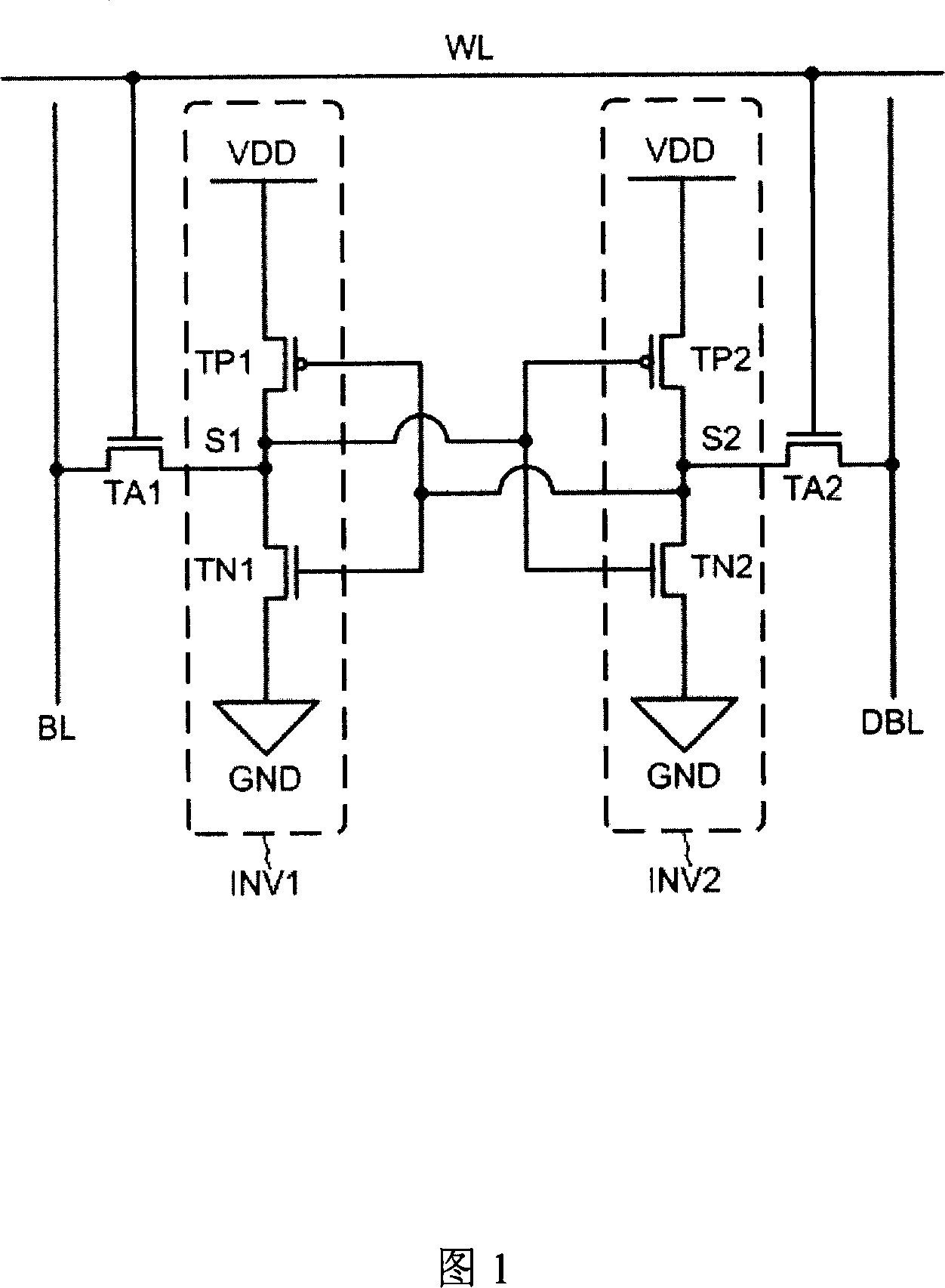
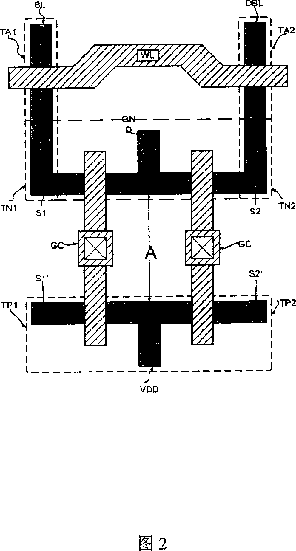
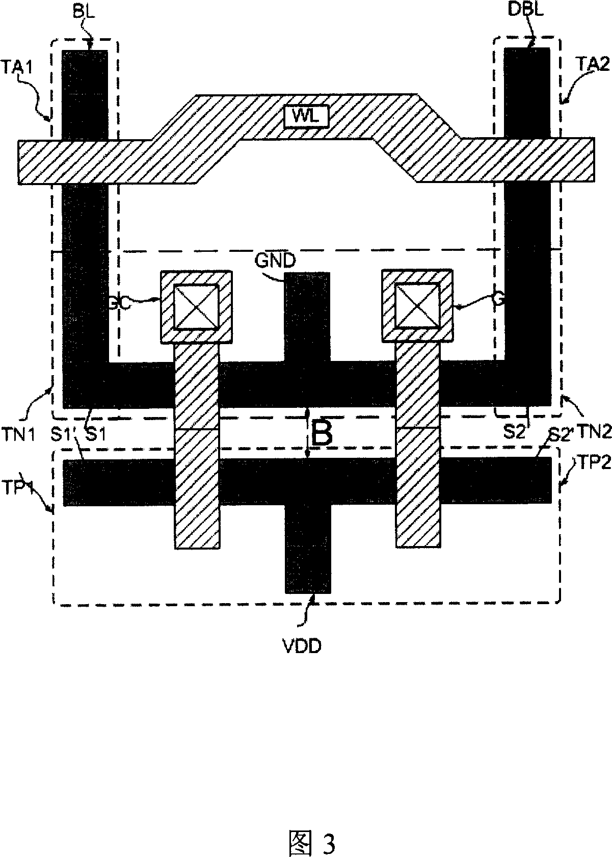
[0047] Now referring to FIGS. 4 , 5 and 6 , the specific embodiment of the present invention will be described. The present invention is a complete CMOS PDSOI SRAM cell that can eliminate the floating body effect.

[0048] First, an SOI substrate is prepared, includin...


PUM


Abstract

This invention relates to a static random access memory, and more specifically, the SRAM formed in PD SOI substrate and its production method. The SRAM unit is six-transistor memory unit, the first, second access NMOS transistors, the first, second drive NMOS transistors, the first, second load PMOS transistors. Among them, the access NMOS transistors and the load PMOS transistors uses the T-type grid contact, and the drive NMOS uses BTS-A grid contact. The leakage of the access NMOS transistors and the drive NMOS transistors connect each other in a common area. The six transistors are all formed in PD SOI substrate, and all processed the body area contact, not only to avoid bolt-lock effect of the bulk silicon devices, but also to basically eliminate the floating body effect caused by the PD SOI substrate, and it enhances the final performance of the chip.

Description

technical field [0001] The invention relates to a static random access memory (SRAM), more specifically, a static random access memory formed on a PDSOI substrate and a manufacturing method thereof. Background technique [0002] According to the data storage method, semiconductor memory is divided into dynamic random access memory (DRAM), non-volatile memory and static random access memory (SRAM). SRAM has established its unique advantage by being able to achieve fast operating speeds in a simple and low power consumption manner. Also, compared to DRAM, SRAM is relatively easy to design and manufacture because it does not need to periodically refresh the stored information. [0003] Typically, an SRAM cell consists of two drive transistors, two load devices, and two access transistors. According to the type of load device contained, SRAM itself can be divided into complete CMOS SRAM, high load resistance (High Load Resistor) SRAM and thin film transistor (Thin FilmTransist...

Claims


Application Information

Patent Timeline
IPC IPC(8): H01L27/11H01L21/8244G11C11/413
Inventor 赵凯刘忠立姜凡
Owner INST OF SEMICONDUCTORS - CHINESE ACAD OF SCI
Why Eureka
Try Eureka