Methodology to reduce SOI floating-body effect

a floating body effect and soi technology, applied in the field of soi mosfet floating body effect control, can solve the problems of short channel effect, less than ideal sub-threshold voltage rolloff, and increasing apparent disadvantages of bulk mosfets

Inactive Publication Date: 2008-08-12
NORTH STAR INNOVATIONS
View PDF14 Cites 29 Cited by
  • Summary
  • Abstract
  • Description
  • Claims
  • Application Information

AI Technical Summary

Problems solved by technology

However, as MOSFET devices have continued to shrink in size, and as the transistor densities in these devices have increased accordingly, the disadvantages associated with bulk MOSFETs have become increasingly apparent.
These disadvantages include an often less than ideal sub-threshold voltage rolloff, short channel effects, drain induced barrier lowering, high junction capacitance, ineffec

Method used


Image

  • Methodology to reduce SOI floating-body effect
  • Methodology to reduce SOI floating-body effect
  • Methodology to reduce SOI floating-body effect

Examples


Embodiment Construction

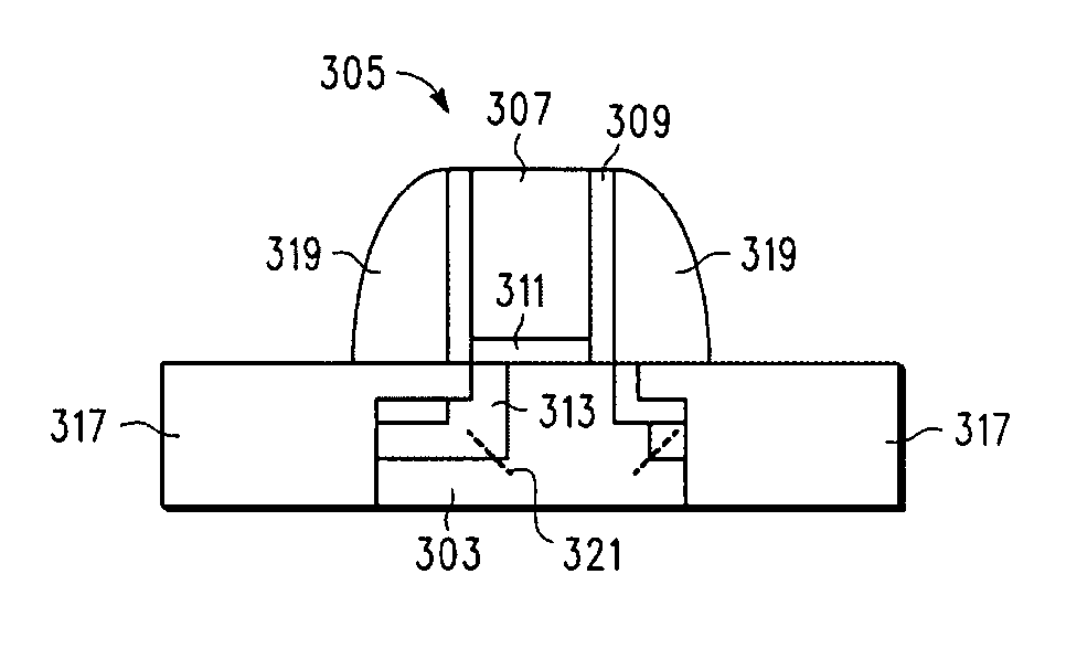
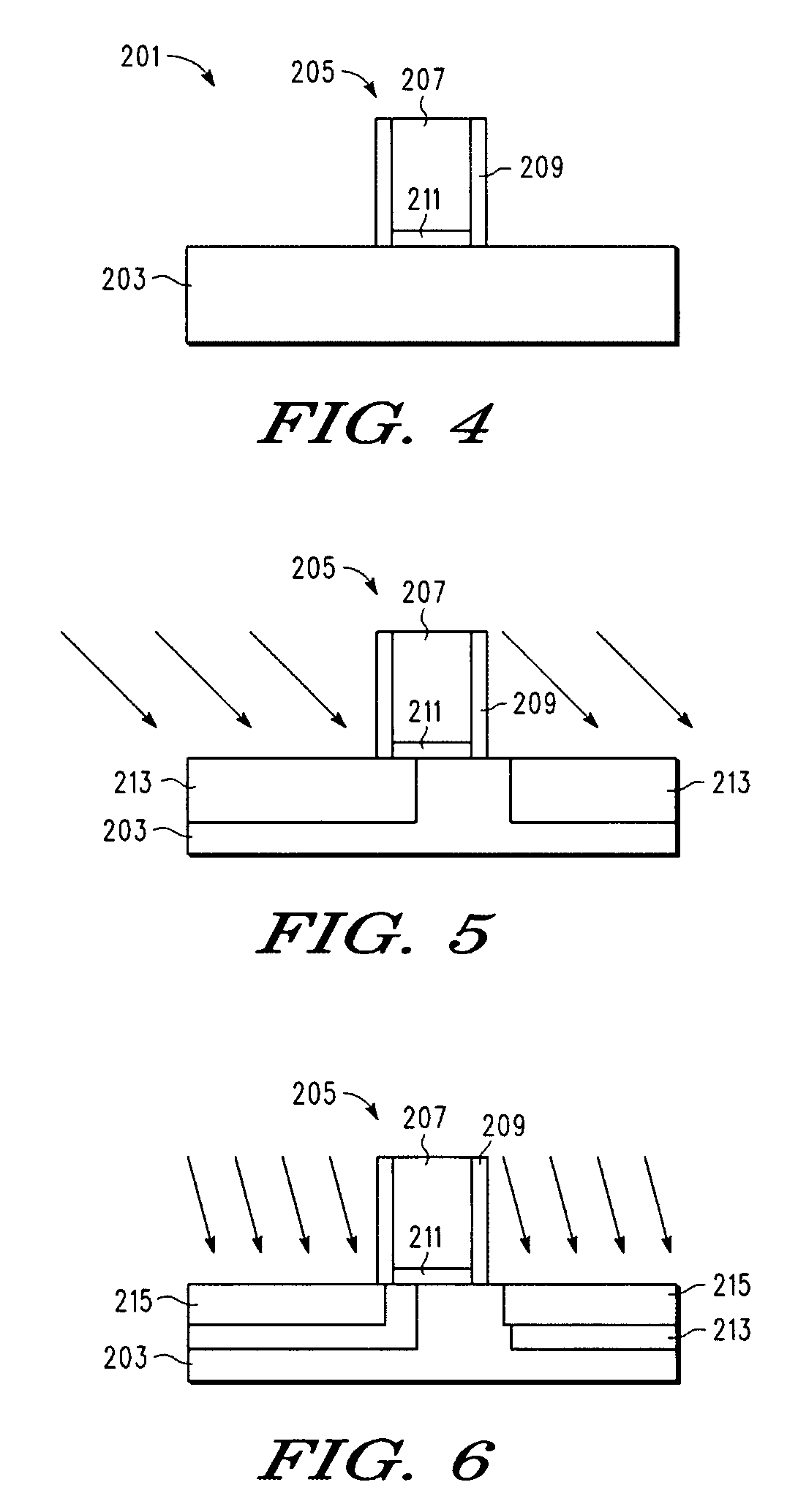
[0021]In one aspect, a method for making a semiconductor device is provided. In accordance with the method, a structure is provided which comprises a gate electrode disposed on a substrate. First and second pre-amorphization implant regions are created in the substrate such that the first and second pre-amorphization implant regions are asymmetrically disposed with respect to said gate electrode. First and second spacer structures are created adjacent to first and second sides of the gate electrode such that the first and second spacer structures overlap the first and second pre-amorphization implant regions, respectively. Source and drain regions are then created in the substrate adjacent, respectively, to the first and second spacer structures.

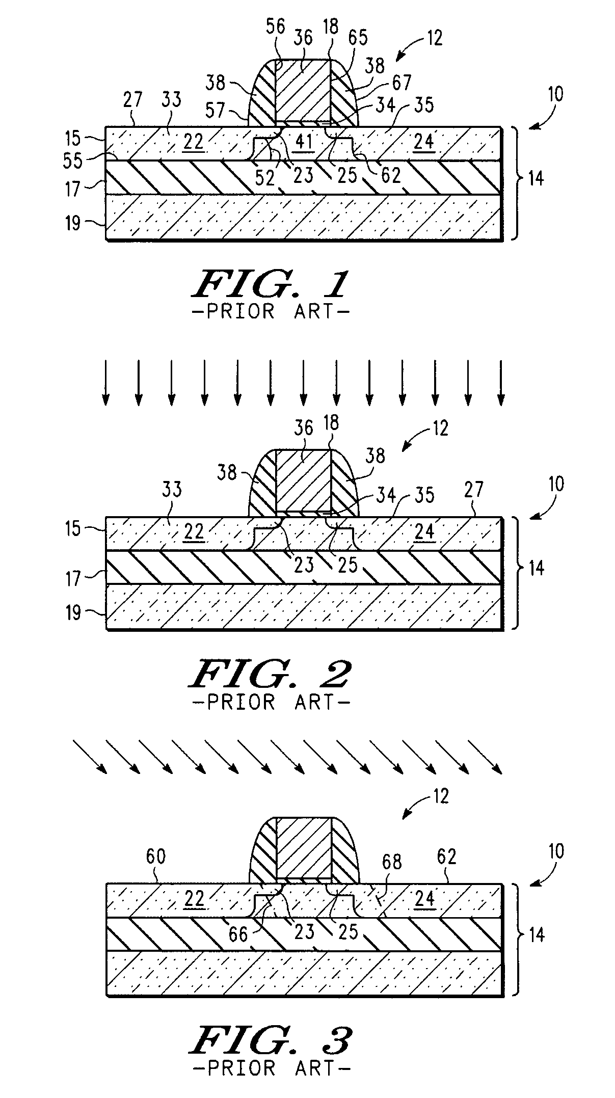
[0022]Without wishing to be bound by theory, the floating-body effect is believed to be caused by impact ionization in the channel region during on-state operation. Such impact ionization typically occurs near the drain side of the channel r...


PUM


Abstract

A method for making a semiconductor device, comprising (a) providing a structure comprising a gate electrode (207) disposed on a substrate (203); (b) creating first (213) and second (214) pre-amorphization implant regions in the substrate such that the first and second pre-amorphization implant regions are asymmetrically disposed with respect to said gate electrode; (c) creating first (219) and second (220) spacer structures adjacent to first and second sides of the gate electrode, wherein the first and second spacer structures overlap the first and second pre-amorphization implant regions; and (d) creating source (217) and drain (218) regions in the substrate adjacent, respectively, to the first and second spacer structures.

Description

FIELD OF THE DISCLOSURE[0001]The present disclosure relates generally to semiconductor devices built on SOI layers, and more particularly to methods for controlling the floating body effect in SOI MOSFETs.BACKGROUND OF THE DISCLOSURE[0002]In the past, Metal Oxide Semiconductor Field Effect Transistors (MOSFETs) were frequently fabricated as bulk semiconductor devices in which the device features were defined on the surface of a bulk semiconductor wafer. However, as MOSFET devices have continued to shrink in size, and as the transistor densities in these devices have increased accordingly, the disadvantages associated with bulk MOSFETs have become increasingly apparent. These disadvantages include an often less than ideal sub-threshold voltage rolloff, short channel effects, drain induced barrier lowering, high junction capacitance, ineffective isolation, and low saturation current.[0003]As a result, many MOSFET devices today are fabricated on Semiconductor-On-Insulator (SOI) wafers ...

Claims


Application Information

Patent Timeline
IPC IPC(8): H01L21/336H01L21/425H01L21/84
CPCH01L21/26506H01L21/26586H01L29/1083H01L29/78624H01L29/66772H01L29/7835H01L29/78612H01L29/66659H01L29/6656H01L21/2658
Inventor MIN, BYOUNG W.CHEEK, JON D.KOLAGUNTA, VENKAT R.
Owner NORTH STAR INNOVATIONS
Why Eureka
Try Eureka