Hybrid bulk-SOI 6T-SRAM cell for improved cell stability and performance

a cell stability and performance improvement technology, applied in the field of semiconductor devices, can solve the problems of reducing the stability of certain circuit array cell structures, negating the favorable effect of adaptive well biasing, and affecting the stability of certain circuit array cells, such as the commonly used 6t sram cell,

Active Publication Date: 2007-09-25
GLOBALFOUNDRIES US INC
View PDF0 Cites 33 Cited by
  • Summary
  • Abstract
  • Description
  • Claims
  • Application Information

AI Technical Summary

Benefits of technology

[0008]The present invention provides a 6T SRAM cell that includes field effect transistors (FETs) on a SOI substrate region having a device channel capable of being either partially or fully depleted of charge carriers in combination with FETs within a bulk-Si region having a highly doped well body contact which substantially eliminates floating body effects and provides a means to use adaptive well biasing thereby providing a means to control the threshold voltages of the bulk-Si region FETs with an applied bias on the well terminal.
[0009]The present invention combines the use of the HOT structure with devices in the 6T-SRAM array. A highly doped well is created and contracted for the device type located in the bulk-Si region. The floating body effect is then eliminated for the FETs placed in the bulk-Si region and the array performance and stability is improved, as the need to raise the linear Vt value, as in a conventional SOI 6T-SRAM cell, is eliminated. Additionally, the well or body node provides the means for applying a bias to implement the adaptive well biasing technique for the devices placed in the conventional bulk CMOS region. Additionally, because the well is unipolar, there are no well to well leakage or capacitance penalties for implementing the adaptive well biasing, which is a major advantage over the conventional bulk CMOS scheme for adaptive well biasing. Adaptive well biasing can be used to either reduce the power consumption of the array or increase the array performance dynamically as needed by the circuit application.
[0017]In accordance with the present invention, the second device within the bulk-Si region can be formed by implanting the bulk-Si region with a first type dopant to provide a well region, forming at least one gate region atop a surface of the bulk-Si region, forming source and drain regions adjacent at least one gate region with a second type dopant, and forming a contact to the well region, wherein the contact stabilizes floating body effects and provides a well contact which may be utilized for adjusting the threshold voltages of the devices in the bulk Si region. Forming the contact to the well region comprises etching a portion of the surface of the bulk-Si region to provide a via to the well region; and filling the via to the well region with a conductive material.
[0018]In accordance with the present invention, selected devices in a six transistor static random access memory (6T-SRAM) are placed in the bulk-Si region while leaving the other transistors in the SOI region. Specifically, four cases are considered (See (a)-(d) above). In the first case, only the two nFET pass-gate devices, or access devices, are placed in the bulk-Si region. In the second case, both the two-pass nFET gate devices and the two pull-down nFET devices are in the bulk-Si region. In the third case, only the two pull-down nFET devices are in the bulk-Si region. In these three cases, the bulk region crystallographic orientation would mostly likely be (100) for optimal nFET device performance. In the fourth and final case, both pull-up pFET devices would be in the bulk-Si region. In the forth case, the bulk region crystallographic orientation would mostly likely be (110) or (111) for optimal nFET device performance in a silicon device. More generally, in other semiconductor material systems (such as other group IV elements, and group III-V and II-VI compounds), the HOT process enables the optimal crystallographic orientation to be used for nFET and pFET devices. The same issues for floating body SOI versus bulk devices would apply for these cases as well.

Problems solved by technology

A drawback in some SOI circuits is the floating body effect.
In principal, body tie structures may be employed in SOI CMOS to add a contact to the floating body node, but this introduces parasitic resistances and capacitances which would negate the favorable impact of adaptive well biasing.
However, certain circuit array cell stability, such as the commonly used 6T SRAM cell, is degraded due to tolerance issues arising from the floating body.
This is typically handled with increasing the linear threshold voltage (Vt) of the FETs in the array, but this is usually at the cost of lowering the overall array performance.

Method used


Image

  • Hybrid bulk-SOI 6T-SRAM cell for improved cell stability and performance
  • Hybrid bulk-SOI 6T-SRAM cell for improved cell stability and performance
  • Hybrid bulk-SOI 6T-SRAM cell for improved cell stability and performance

Examples


Embodiment Construction

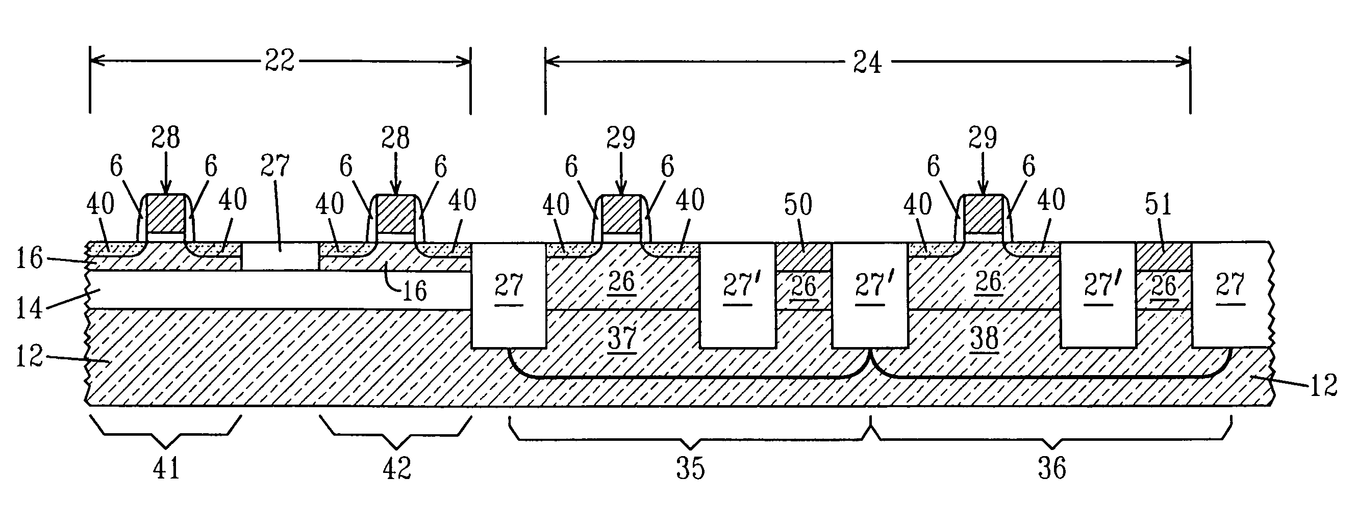
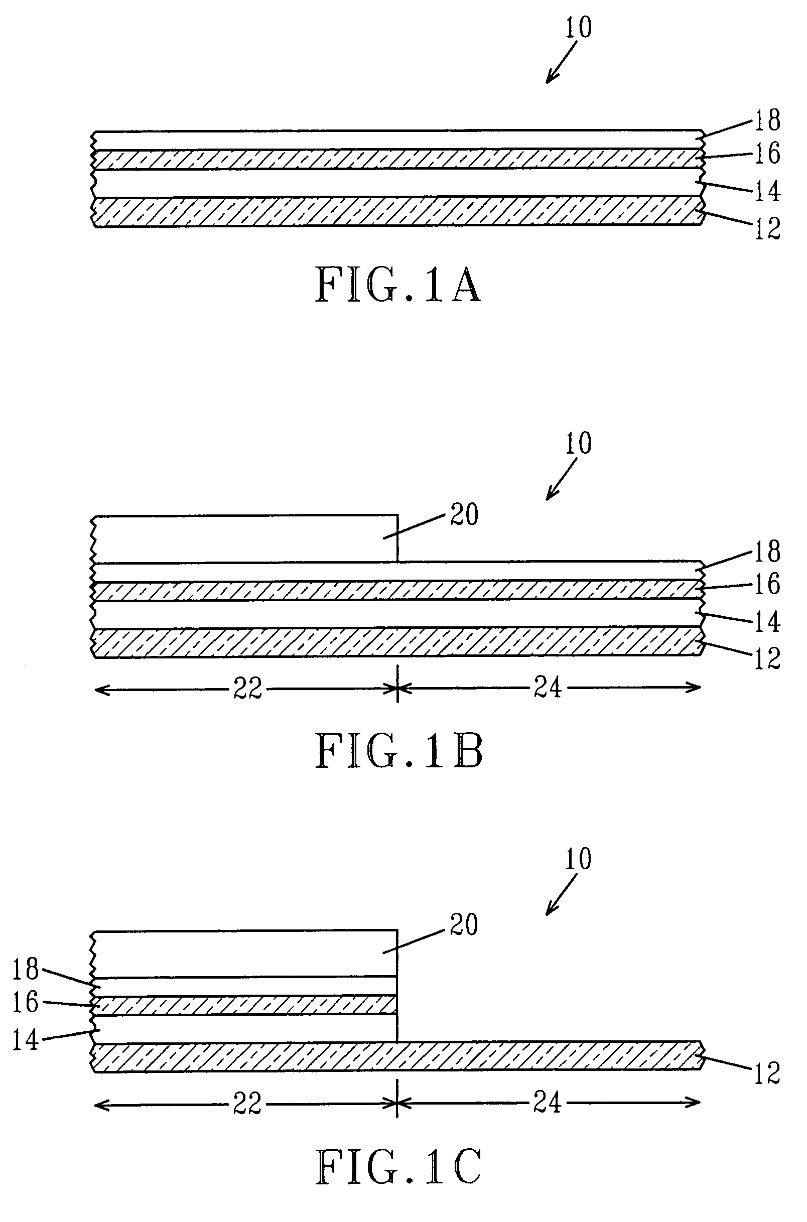
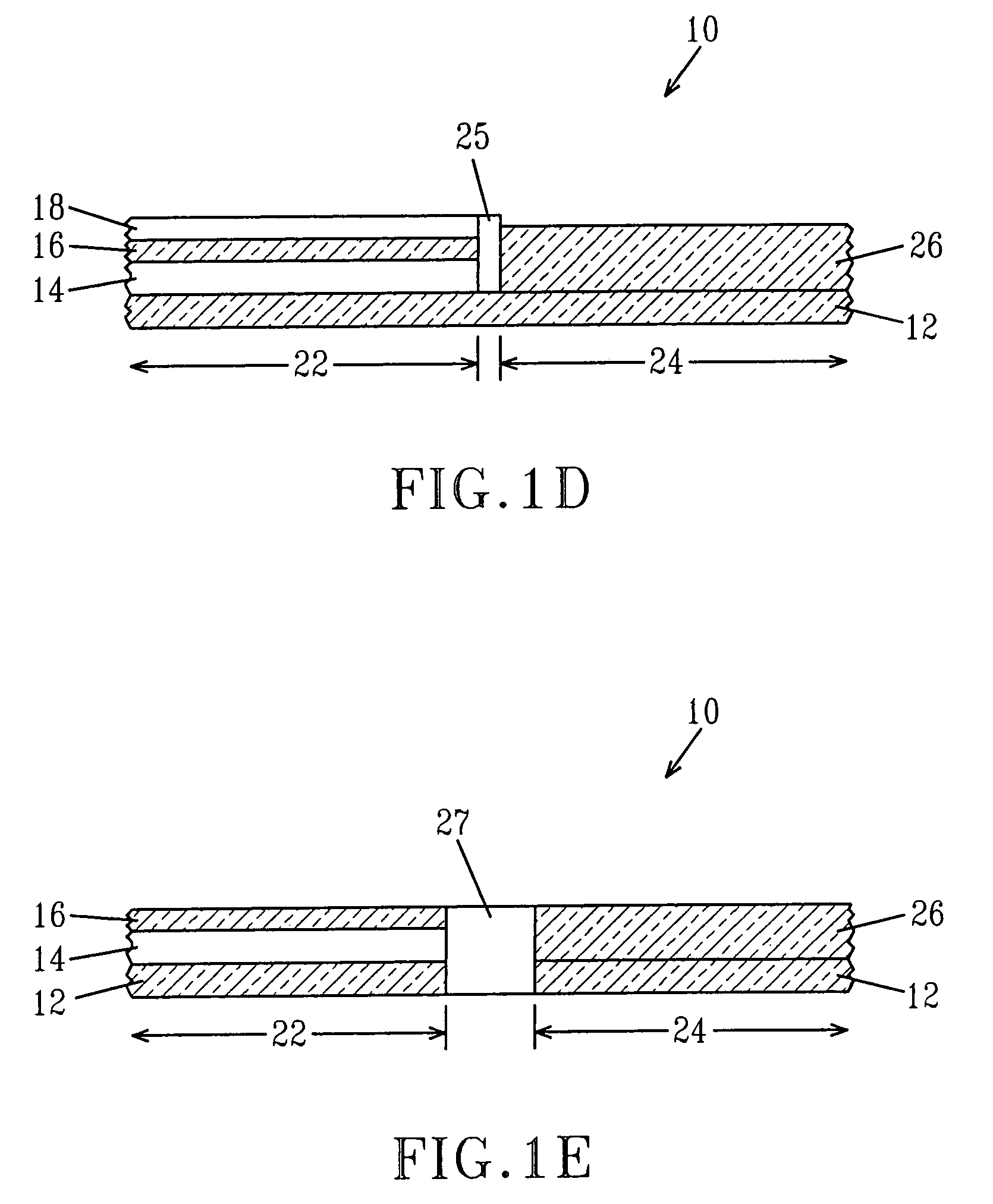
[0023]The present invention, which provides a method for increasing the SRAM cell stability and performance in a hybrid bulk-SOI technology over that of a conventional SOI technology, will now be described in greater detail by referring to the following discussion as well as the drawings that accompany the present application. In the accompanying drawings, like and correspondence elements are referred to by like reference numerals. It is noted that the drawings of the present invention are provided for illustrative purposes and thus they are not drawn to scale.

[0024]FIG. 1A illustrates a substrate 10, i.e., hybrid substrate, which may be employed in the present invention. As shown, the substrate 10 includes a surface dielectric layer 18, a first semiconductor layer 16, an insulating layer 14, and a second semiconductor layer 12.

[0025]The surface dielectric layer 18 of the substrate 10 is an oxide, nitride, oxynitride or other insulating layer that is either present in one of the ini...


PUM


Abstract

The present invention provides a 6T-SRAM semiconducting structure including a substrate having an SOI region and a bulk-Si region, wherein the SOI region and the bulk-Si region have a same or differing crystallographic orientation; an isolation region separating the SOI region from the bulk-Si region; and at least one first device located in the SOI region and at least one second device located in the bulk-Si region. The SOI region has an silicon layer atop an insulating layer. The bulk-Si region further comprises a well region underlying the second device and a contact to the well region, wherein the contact stabilizes floating body effects. The well contact is also used to control the threshold voltages of the FETs in the bulk-Si region to optimized the power and performance of the SRAM cell built from the combination of the SOI and bulk-Si region FETs.

Description

FIELD OF THE INVENTION[0001]The present invention relates to semiconductor devices, and more particularly to integrated semiconductor devices, such as complementary metal oxide semiconductor (CMOS) devices formed atop a substrate having thin silicon-on-insulator (SOI) and bulk-Si portions, wherein the SOI and bulk-Si portions of the substrate have either the same or differing crystalline orientation. In particular, the present invention forms nFET and pFET devices on SOI and bulk-Si regions of a semiconducting substrate having either a surface on a (100), (110), or (111) crystal plane. The bulk-Si region of the substrate may also be processed to provide devices substantially free of floating body effects that are typically present in the devices formed with SOI substrates. More specifically, the present invention relates to a 6T-SRAM (six transistor static random access memory) cell that has improved stability and performance.BACKGROUND OF THE INVENTION[0002]Silicon-on-insulator (SO...

Claims


Application Information

Patent Timeline
Patent Type & Authority Patents(United States)
IPC IPC(8): H01L29/72
CPCG11C11/412H01L21/84H01L27/1207H01L27/1104H01L27/1203H01L27/11H10B10/00H10B10/12
Inventor CHANG, LELANDNARASIMHA, SHREESHROHRER, NORMAN J.SLEIGHT, JEFFREY W.
Owner GLOBALFOUNDRIES US INC
Why Eureka
Try Eureka