Soi field effect transistor having asymmetric junction leakage

Inactive Publication Date: 2009-02-05
GLOBALFOUNDRIES INC
View PDF2 Cites 29 Cited by
  • Summary
  • Abstract
  • Description
  • Claims
  • Application Information

AI Technical Summary

Benefits of technology

[0008]According to the present invention, an asymmetric disposable spacer is formed on sidewalls of a gate conductor formed on a top semiconductor layer comprising a first semiconductor material in a semiconductor substrate. The asymmetric disposable spacer has a narrower width on a source side than on a drain side. Exposed portions of a top semiconductor layer are etched to form a source trench and a drain trench. A second semiconductor material having a narrower band gap than the first semiconductor material is deposited in the source trench and the drain trench to form a source side narrow band gap region and a drain side narrow band gap region, respectively. Preferably, the second semiconductor material is formed epitaxially on the remaining first semiconductor material in the top semiconductor layer. Selective epitaxy may be employed to avoid formation of the second semiconductor material on dielectric surfaces. The asymmetric dis

Problems solved by technology

However, a MOSFET built on an SOI substrate tends to have less consistency in the device operation due to “history effect,” or “floating body effect,” in which the potential of the body, and subsequently, the timing of the turn-on and the on-current of the SOI MOSFET are dependent on the past history of the SOI MOSFET.
Furthermore, the level of leakage current also depends on the voltage of the floating body, which poses a challenge in the design of a low power SOI MOSFET.
As such, SOI MOSFETs exhibit threshold voltages which are difficult to anticipat

Method used


Image

  • Soi field effect transistor having asymmetric junction leakage
  • Soi field effect transistor having asymmetric junction leakage
  • Soi field effect transistor having asymmetric junction leakage

Examples


Embodiment Construction

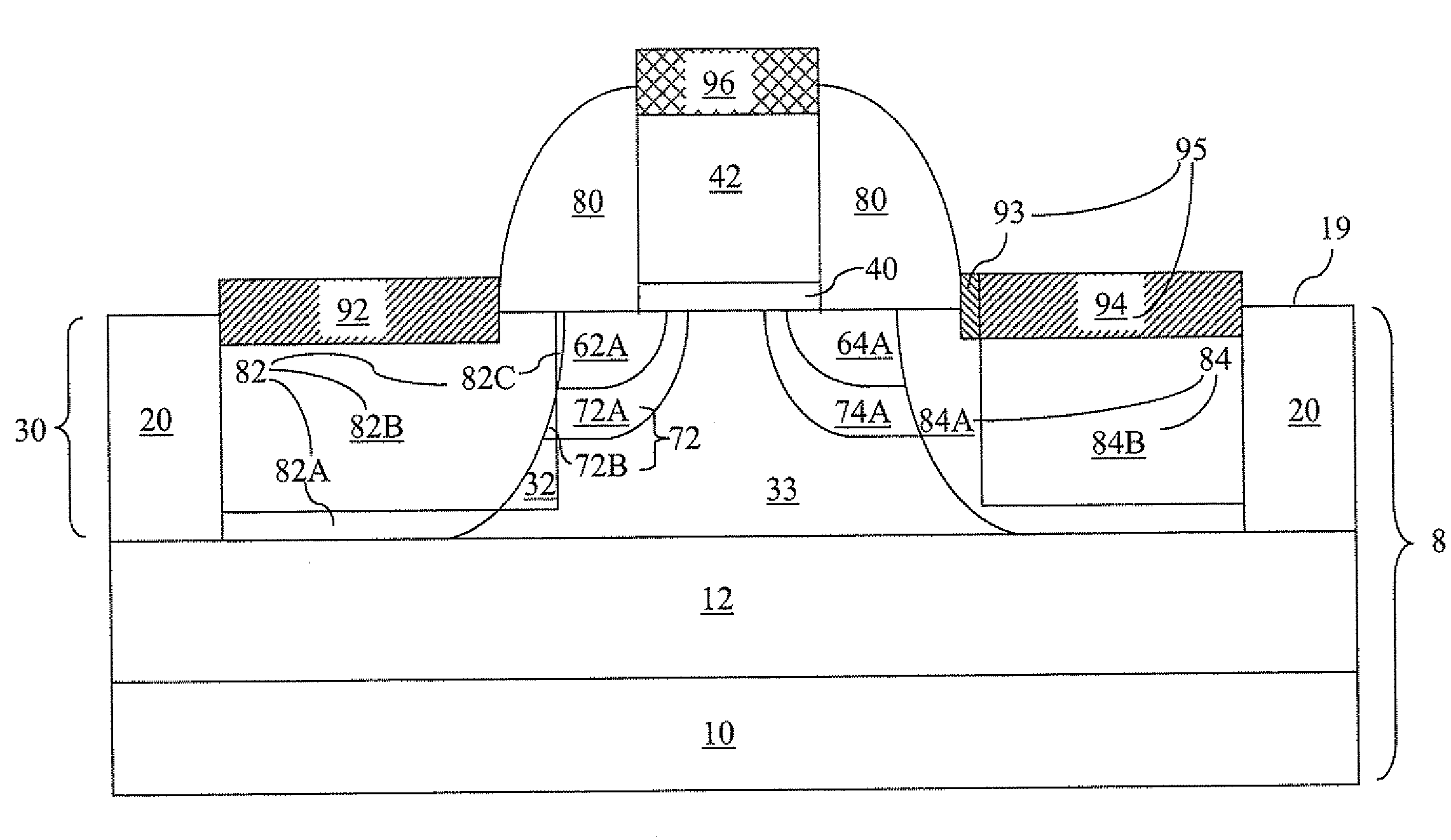
[0049]As stated above, the present invention relates to a semiconductor-on-insulator (SOI) metal oxide semiconductor field effect transistor (MOSFET) having asymmetric junction leakage and methods of manufacturing the same, which are now described in detail with accompanying figures. It is noted that like and corresponding elements are referred to by like reference numerals.

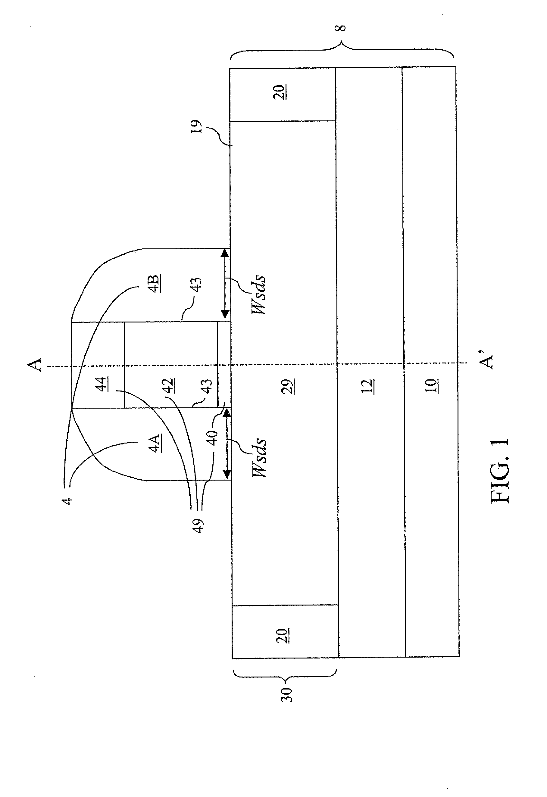
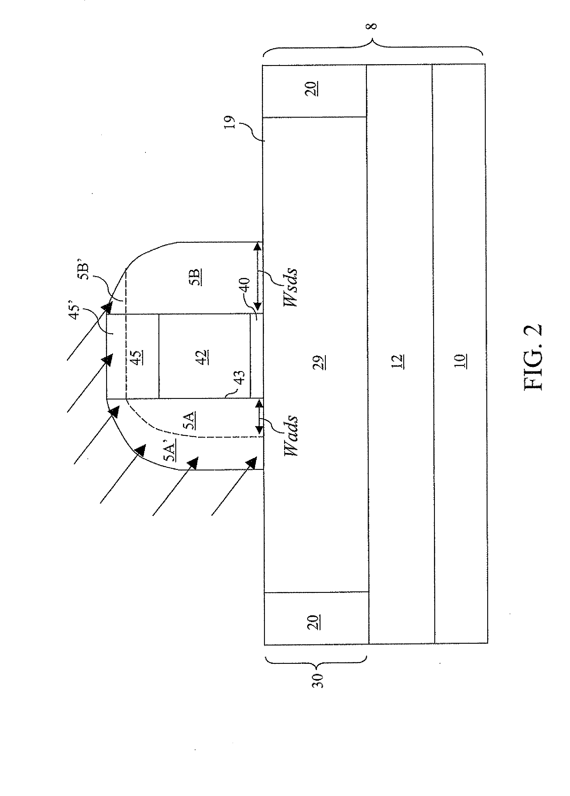
[0050]Referring to FIG. 1, a first exemplary semiconductor structure according to the present invention comprises an SOI substrate 8 containing a handle substrate 10, a buried oxide layer 12, and a top semiconductor layer 30. The top semiconductor layer 30 contains shallow trench isolation 20 comprising a dielectric material and a semiconductor region 29 comprising a semiconductor material. The shallow trench isolation 20 abuts the buried insulator layer 12 and laterally surrounds the semiconductor region 29 so that the semiconductor region 29 is electrically isolated from other semiconductor regions (not shown) ...


PUM


Abstract

A source trench and a drain trench are asymmetrically formed in a top semiconductor layer comprising a first semiconductor in a semiconductor substrate. A second semiconductor material having a narrower band gap than the first semiconductor material is deposited in the source trench and the drain trench to form a source side narrow band gap region and a drain side narrow band gap region, respectively. A gate spacer is formed and source and drain regions are formed in the top semiconductor layer. A portion of the boundary between an extended source region and an extended body region is formed in the source side narrow band gap region. Due to the narrower band gap of the second semiconductor material compared to the band gap of the first semiconductor material, charge formed in the extended body region is discharged through the source and floating body effects are reduced or eliminated.

Description

FIELD OF THE INVENTION[0001]The present invention relates to semiconductor devices, and particularly, to a semiconductor-on-insulator (SOI) metal oxide semiconductor field effect transistor (MOSFET) having asymmetric junction leakage and methods of manufacturing the same.BACKGROUND OF THE INVENTION[0002]Metal oxide semiconductor field effect transistors (MOSFETs) built on a semiconductor-on-insulator (SOI) substrate in general offer advantages over a MOSFET with comparable dimensions that is built on a bulk substrate by providing a higher on-current and lower parasitic capacitance between the body and other MOSFET components. However, a MOSFET built on an SOI substrate tends to have less consistency in the device operation due to “history effect,” or “floating body effect,” in which the potential of the body, and subsequently, the timing of the turn-on and the on-current of the SOI MOSFET are dependent on the past history of the SOI MOSFET. Furthermore, the level of leakage current ...

Claims


Application Information

Patent Timeline
IPC IPC(8): H01L29/778H01L21/336
CPCH01L21/26506H01L29/78654H01L29/1045H01L29/1083H01L29/165H01L29/205H01L29/26H01L29/267H01L29/4966H01L29/665H01L29/6653H01L29/66537H01L29/6659H01L29/66636H01L29/66659H01L29/66772H01L29/7835H01L29/7843H01L21/26586
Inventor ZHU, HUILONGLUO, ZHIJIONGLIANG, QINGQING
Owner GLOBALFOUNDRIES INC
Why Eureka
Try Eureka