Method for manufacturing antenna and method for manufacturing semiconductor device

a manufacturing method and antenna technology, applied in the manufacture of printed circuits, solid-state devices, basic electric elements, etc., can solve the problems of increasing the number of steps for forming antennas, reducing communication distances, and requiring a lot of processing time, so as to reduce antenna resistance, increase antenna width, and increase the number of windings

Inactive Publication Date: 2006-11-30
SEMICON ENERGY LAB CO LTD
View PDF6 Cites 61 Cited by
  • Summary
  • Abstract
  • Description
  • Claims
  • Application Information

AI Technical Summary

Benefits of technology

[0026] In the present invention, since an antenna is formed by being irradiated with a laser, a width between lines of the antenna can be reduced to 20±5 μm, which can be dramatically narrower than that of an antenna formed by a conventional method without using a mask. Therefore, when an antenna is formed in a predetermined area, a width of the antenna can be increased or the winding number can be increased, making it possible to reduce resistance of the antenna and improve a communication distance of a wireless chip. Further, since processing time required for forming an antenna can be drastically shortened as compared with a method by which an object is patterned by using a mask made from a resist, throughput is improved. Moreover, a substrate having a surface with concavity and convexity or a substrate having a curved surface can be used as an object (a substrate) over which an antenna is formed in addition to a substrate having a flat surface, and therefore, there are high expectations for its application in various industrial fields in addition to the semiconductor field. In this specification, “patterning” indicates treatment by which an object is etched into a desired shape.

Problems solved by technology

Therefore, there is a concern that as increasing the resistance (R) of an antenna, the Q value is reduced, which results in reduction in a communication distance.
However, this method has problems that since the mask made from a resist is used, the number of steps for forming an antenna is increased so that lots of processing time is required.
In addition, manufacturing cost is also increased with increasing the number of steps and processing time.
Accordingly, a width of an antenna cannot be sufficiently widened and resistance of the antenna is increased; and therefore, it has been difficult to improve a communication distance.
Further, in a case of forming a loop antenna as an antenna, the sufficient winding number cannot be secured so that it has been difficult to manufacture a semiconductor device with a sufficient communication distance.

Method used


Image

  • Method for manufacturing antenna and method for manufacturing semiconductor device
  • Method for manufacturing antenna and method for manufacturing semiconductor device
  • Method for manufacturing antenna and method for manufacturing semiconductor device

Examples


embodiment modes

[0044] The embodiment modes of the present invention will be described below. It is easily understood by those skilled in the art that the embodiment modes and details herein disclosed can be modified in various ways without departing from the purpose and the scope of the invention. The present invention should not be interpreted as being limited to the description of the embodiment modes to be given below. Further, in the structure of the present invention, reference numerals indicating the same things are commonly used in the drawings.

embodiment mode 1

[0045] In this embodiment mode, an example of a method for manufacturing a semiconductor device of the present invention will be described with reference to the drawings.

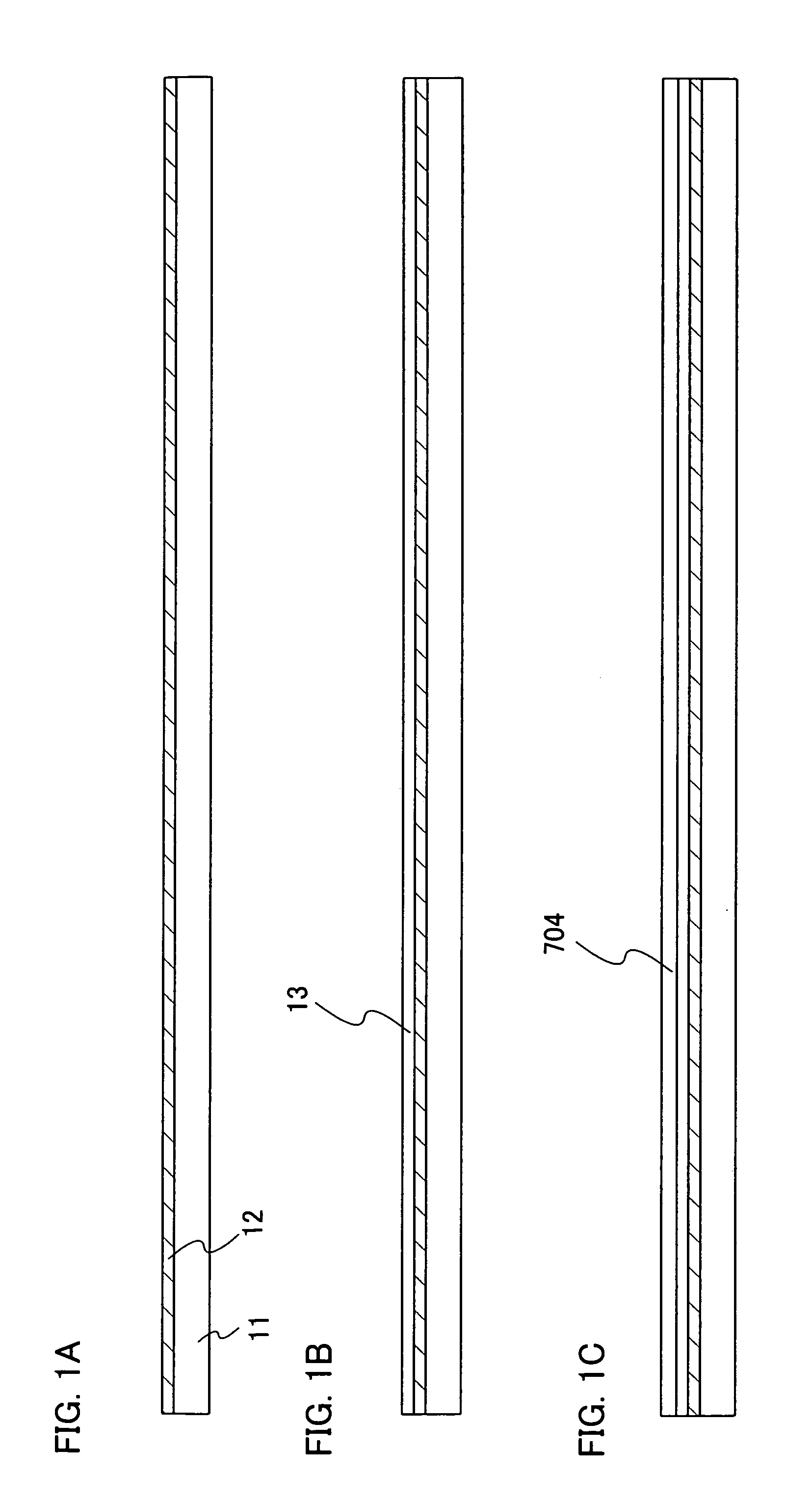
[0046] First, a separation layer 12 is formed over a surface of a substrate 11 (FIG. 1A).

[0047] The substrate 11 is removed in the subsequent step, and can be formed using a glass substrate, a quartz substrate, a ceramic substrate, or the like. Further, a metal substrate containing stainless steel, a silicon substrate, or a semiconductor substrate having a surface over which an insulating film is formed, may also be used as the substrate 11. Furthermore, a flexible substrate typified by a synthetic resin such as acrylic can be used. Preferably, a glass substrate, a plastic substrate (for example, an acrylic substrate) having a heat resistance property, which can withstand heating treatment in a process of manufacturing a semiconductor device, or the like may be used. As the plastic substrate having the heat resist...

embodiment mode 2

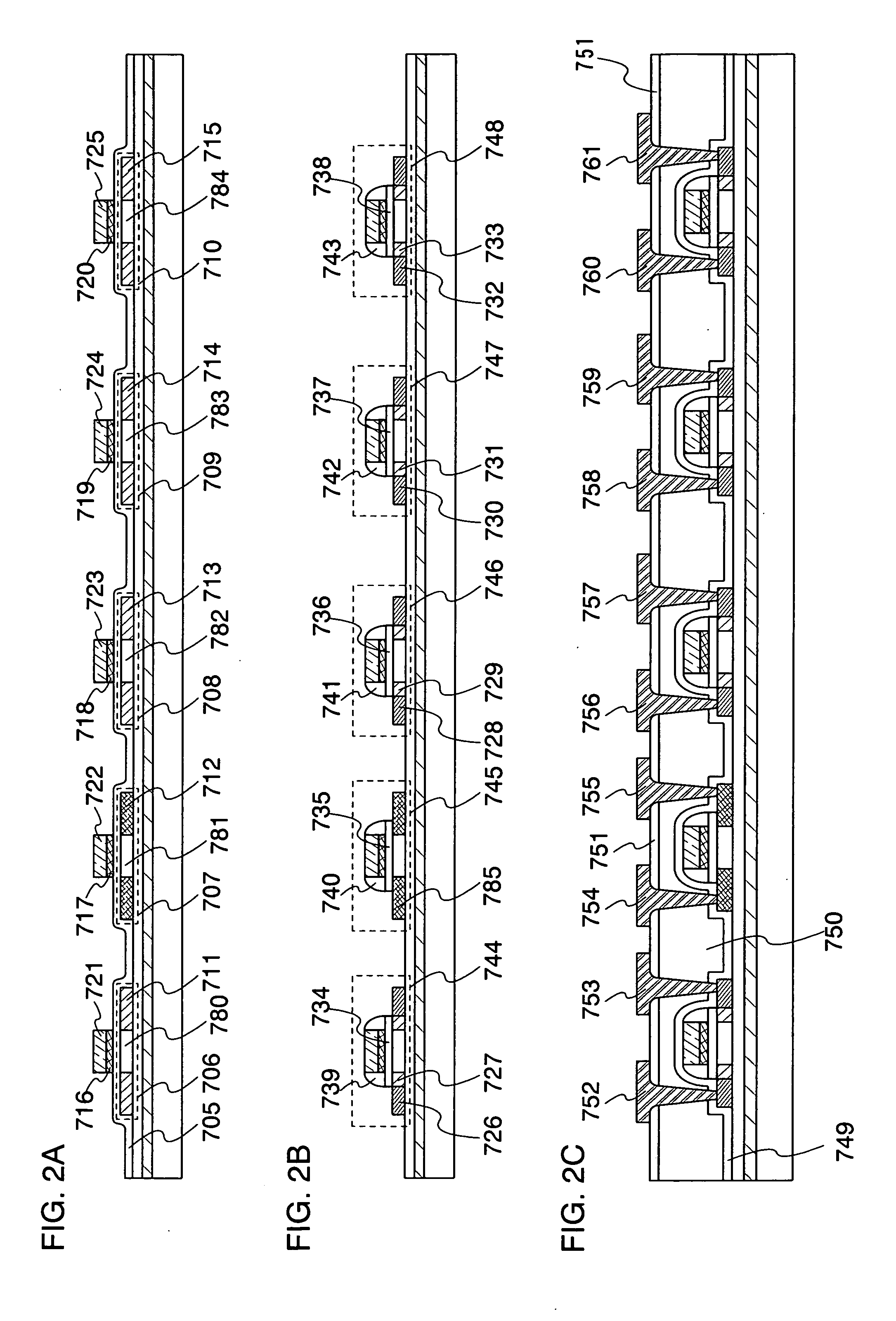
[0114] In this embodiment mode, a method for manufacturing a semiconductor device, which is different from the method described in Embodiment Mode 1, will be described with reference to the drawings.

[0115] Although a case of forming the antenna in the interior portion of the element layer along with the thin film transistors, is described in Embodiment Mode 1, a method for forming a semiconductor device where an antenna is separately formed from thin film transistors and then the antenna and the thin film transistors are electrically connected to each other, will be described in this embodiment mode.

[0116] First, a substrate over which an antenna is provided, is previously formed. A method for forming the substrate over which the antenna is provided, will be described below.

[0117] A conductive film is formed over a substrate 235 by coating. Alternatively, in order to prevent part of a substrate 235 from being etched in patterning the conductive film by laser irradiation in a subs...


PUM

PropertyMeasurementUnit
wavelengthaaaaaaaaaa
widthaaaaaaaaaa

Abstract

The present invention provides an antenna with low resistance and a semiconductor device having an antenna whose communication distance is improved. A fluid containing conductive particles is applied over an object. After curing the fluid containing the conductive particles, the fluid is irradiated with a laser to form an antenna. As a method for applying the fluid containing the conductive particles, screen printing, spin coating, dipping, or a droplet discharging method is used. Further, a solid laser having a wavelength of 1 nm or more and 380 nm or less is used as the laser.

Description

BACKGROUND OF THE INVENTION [0001] 1. Field of the Invention [0002] The present invention relates to a method for manufacturing an antenna. Moreover, the present invention relates to a method for manufacturing a semiconductor device having an antenna. [0003] 2. Description of the Related Art [0004] In recent years, development of a semiconductor device which can send and receive data wirelessly has been actively carried out. Such a semiconductor device is also referred to as an IC tag, an ID tag, an RF (radio frequency) tag, an RFID (radio frequency identification) tag, a wireless tag, an electronic tag, a wireless processor, a wireless memory, a wireless chip, or the like. [0005] A wireless chip generally includes an antenna and an IC chip. The IC chip is formed using an element layer having a transistor and the like provided over a silicon wafer. [0006] As one of characteristics required for an antenna of a wireless chip, there is low resistance of an antenna (a wiring) itself. Th...

Claims


Application Information

Patent Timeline
Patent Type & Authority Applications(United States)
IPC IPC(8): H01L21/20
CPCH01L21/6835H01L21/6836H01L2924/00011H01L2224/293H01L2224/2929H01L27/1292H01L27/1285H01L21/76826H01L21/76856H01L23/5227H01L24/83H01L27/1266H01L27/13H01L2221/68327H01L2221/6834H01L2221/6835H01L2221/68363H01L2223/6677H01L2224/83851H01L2924/09701H01L2924/3011H01L2924/3025H01Q1/2225H05K1/095H05K3/02H01L2924/01067H01L2924/01079H01L2924/01068H01L2924/01012H01L2224/29075H01L2924/00014H01L2924/14H01L2924/00
Inventor AOKI, TOMOYUKIYAMADA, DAIKI
Owner SEMICON ENERGY LAB CO LTD
Why Eureka
Try Eureka