Light source apparatus and optical communication apparatus using the same

a technology of light source apparatus and optical communication apparatus, which is applied in the direction of light source apparatus, solid-state device, free standing, etc., can solve the problems of reducing the size of the light source apparatus itself, the inability of the optical system to always meet industrial needs, and the inability to reduce the size of the light source apparatus. , to achieve the effect of suppressing optical loss, increasing the distance of communication, and increasing the source siz

Inactive Publication Date: 2005-06-09
SHARP KK
View PDF8 Cites 37 Cited by
  • Summary
  • Abstract
  • Description
  • Claims
  • Application Information

AI Technical Summary

Benefits of technology

[0022] According to the optical communication apparatus, distance of communication can be considerably increased compared to the case where a general semiconductor laser is used, which makes it possible to provide an optical communication apparatus applicable to communication between distant locations.
[0023] As is clear from the above description, according to the light source apparatus of the present invention, a small-size and low-cost light source apparatus which ensures a sufficient effect of increasing the source size while suppressing optical loss due to scattering may be implemented by introducing a minute light scattering region.
[0024] According to the optical communication apparatus of the present invention, use of the light source apparatus makes it possible to implement a small-size and low-cost optical communication apparatus capable of expanding communication distance.

Problems solved by technology

Since the actual source size is given as a mean value of the horizontal and vertical values, the size is limited to 0.3 L to 0.9 L. In such a case, increasing the source size requires increasing the distance L from the semiconductor laser chip 101 to the diffuser 110, causing a problem that downsizing of the light source apparatus itself is hindered.
However, in this case, a lens 111 needs to be disposed between a semiconductor laser chip 101 and a diffuser 110, which makes the apparatus even larger, and also due to another factor such as increase in the number of component parts, the optical system does not always satisfy industrial needs.

Method used


Image

  • Light source apparatus and optical communication apparatus using the same
  • Light source apparatus and optical communication apparatus using the same
  • Light source apparatus and optical communication apparatus using the same

Examples


first embodiment

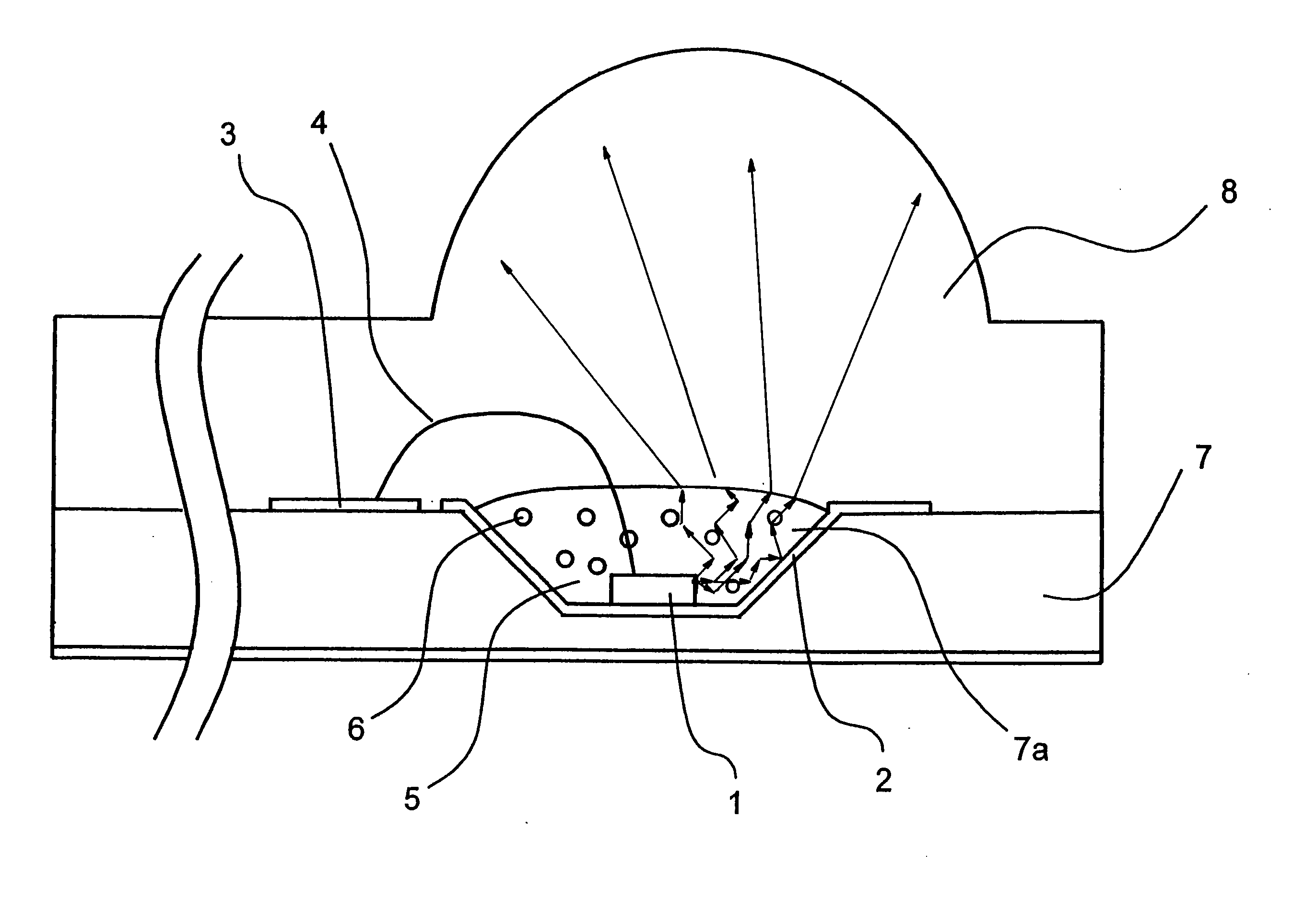
[0074]FIG. 1 is a cross sectional view showing the structure of an optical module as an example of a light source apparatus in a first embodiment of the present invention. Hereinbelow, description is given of the optical module in the first embodiment.

[0075] As shown in FIG. 1, the optical module in the first embodiment is structured such that an inverted cone trapezoid-shaped countersunk hole 7a for disposing a semiconductor laser chip 1 exemplifying the semiconductor laser device is provided on a glass epoxy board 7. On the bottom surface and the inclined surface of the countersunk hole 7a, there is formed a metal reflecting section 2 by gold coating. The metal reflecting section 2 functions as a lower electrode and a light reflecting section of the semiconductor laser chip 1. On the middle portion of the bottom section of the countersunk hole 7a, the semiconductor laser chip 1 is mounted by die-bonding with a conductive paste material. An upper electrode formed on the top surfac...

second embodiment

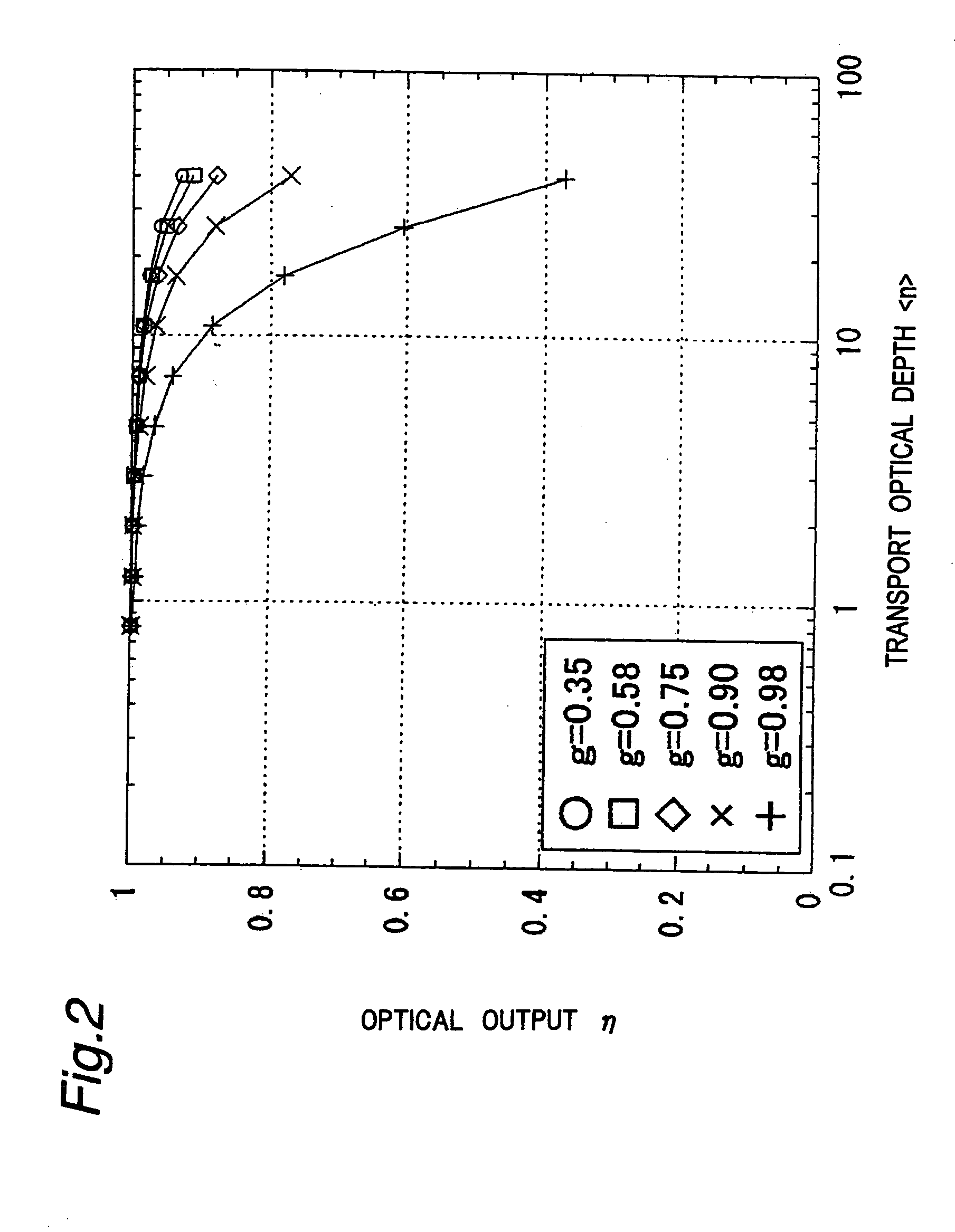
[0084] Description is now given of the optical module as an example of the light source apparatus in a second embodiment of the present invention. The optical module in the second embodiment shares the same structure with the first embodiment except the light scattering region, and therefore FIG. 1 is also used as a reference. In the optical module in the second embodiment, an optimum asymmetry factor g for increasing the source size was obtained by an experiment based on the relation between the asymmetry factor g of the light scattering particles 6 in the light scattering region 5 and the transport optical depth in the light scattering region.

[0085] In the structure of the optical module in the aforementioned first embodiment, it was already proved that the transport optical depth of styrene particles having an asymmetry factor g of 0.75 can be optimized, and therefore it is herein discussed with much circumstance if further increase in source size is possible by using other as...

third embodiment

[0106] Description is now given of an optical module as an example of the light source apparatus in a third embodiment of the present invention. The optical module in the third embodiment shares the same structure with the first embodiment except the light scattering region, and therefore FIG. 1 is also used as a reference. In the optical module in the third embodiment, an optimum asymmetry factor g in the case where consideration is given to an albedo γ which represents the degree of absorption in the light scattering region was obtained by an experiment.

[0107] Description will be given of the result of an experiment in which surface treatment is applied to the light scattering particles 6 in the light scattering region 5 and a certain albedo is given. In this experiment, the particle size of the light scattering particles 6 is unchanged and the value of the asymmetry factor g is the same. In this experiment, the albedo γ is changed in the range of 0.9990 to 0.99997. Two examples ...


PUM


Abstract

A light source apparatus is provided with a light scattering region 5 containing light scattering particles 6 disposed in a part of a region extending from a semiconductor light-emitting laser chip 1 to an external space. An asymmetry factor g of the light scattering particles 6 and a transport optical depth <n> of the light scattering region 5 are set so that their product g.<n> satisfies a following condition:
2≦g·<n>≦40
The light source apparatus is of small-size and low-cost and can ensure safety of human eyes as well as obtain a high optical output.

Description

[0001] This Nonprovisional application claims priority under 35 U.S.C. §119(a) on Patent Applications Nos. P2003-387608 filed in Japan on Nov. 18, 2003, P2004-178328 filed in Japan on Jun. 16, 2004 and P2004-301708 filed in Japan on Oct. 15, 2004, the entire contents of which are hereby incorporated by reference. BACKGROUND OF THE INVENTION [0002] The present invention relates to a light source apparatus and an optical communication apparatus using the same, and more particularly, relates to a light source apparatus applicable to the wide range of consumer technologies including optical wireless communication and light sensor application, and an optical communication apparatus using the same. [0003] Examples of conventional light source apparatuses include one that reduces special coherence of the light emitted from a semiconductor laser device (see, e.g., JP 09-307174 A). In the light source apparatus that reduces special coherence, there is disclosed a method for reducing special ...

Claims


Application Information

Patent Timeline
Patent Type & Authority Applications(United States)
IPC IPC(8): F21S2/00F21V7/04H01L33/54H01L33/56
CPCH01L2933/0091H01L33/56H01L2924/181H01L2224/48091H01L2224/8592H01L2224/45144H01L2924/00014H01L2924/00012H01L2924/00
Inventor SHIMONAKA, ATSUSHIHIRAMATSU, TAKUMA
Owner SHARP KK
Why Eureka
Try Eureka